|
|
|
| 首页 >> CST教程 >> CST2013在线帮助系统 |
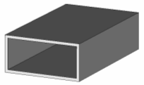
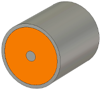
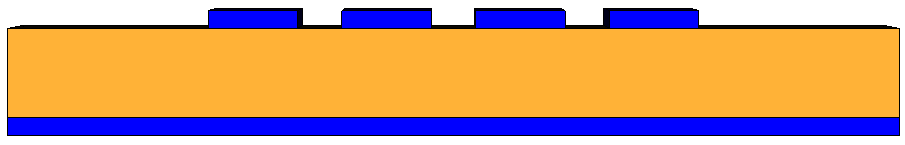
Waveguide Port OverviewWaveguide ports represent a special kind of boundary condition of the calculation domain, enabling the stimulation as well as the absorption of energy. This kind of port simulates an infinitely long waveguide connected to the structure. The waveguide modes travel out of the structure toward the boundary planes thus leaving the computation domain with very low levels of reflections.Very low reflections can be achieved when the waveguide mode patterns in the port match perfectly with the mode patterns from the waveguides inside the structure. CST MICROWAVE STUDIO uses a 2D eigenmode solver to calculate the waveguide port modes. This procedure can provide very low levels of reflection below -100dB in some cases.In general, the definition of a waveguide port requires enclosing the entire field filled domain in the cross section of the transmission line with the port area. The eigenmode solver can then calculate the exact port modes within these boundaries. The number of modes to be considered in the solver calculation can be defined in the waveguide port dialog. The strategies to properly define waveguide ports depend a bit on the type of the transmission line. In the following we focus on the most commonly used applications.Please note that the input signal of an excited waveguide port is normalized to 1 sqrt(Watt) peak power.ContentsInhomogeneous Waveguide Ports (Special Treatment) Microstrip Lines / Coplanar Lines (QTEM Modes) Dielectrically Loaded Waveguides (No QTEM Modes) Waveguide Ports in Hexahedral Mesh View Empty WaveguidesThe most frequently used waveguide type of this category is the rectangular waveguide shown below:
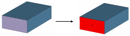
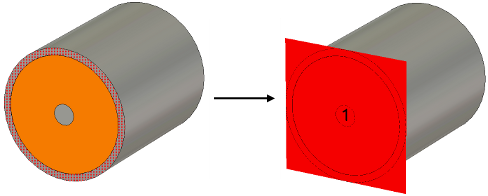
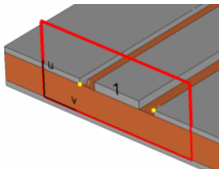
upPort CreationThe port assignment for this type of waveguide is quite simple. However, it is important to make sure that the port covers the entire waveguide cross-section. The easiest way to define a port’s face is to pick structure elements such as points / edges / faces before opening the port definition dialog box. The port dimensions will then automatically adjust to the bounding box of the picked elements. If the interior of the waveguide is modeled by a dielectric material block, you can simply pick the end face of the waveguide as shown in the picture below:
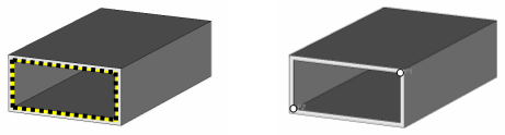
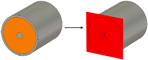
The bounding box of the picked end face will then exactly define the dimension of the port. When the background material is not made of PEC material, it is often required to model the wall of the waveguide, too. For a construction like the one shown in the first picture above, the end face of the rectangular waveguide has not been modeled directly. We therefore recommend to pick the edges on the circumference of the waveguide or to pick two opposite points on the corners:
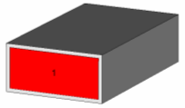
In both cases, the bounding box of the picked elements will be large enough to cover the entire field filled cross-section of the waveguide. The resulting port definition will then look as follows:
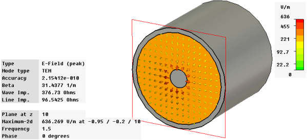
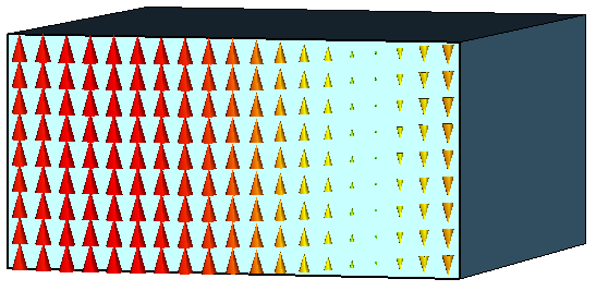
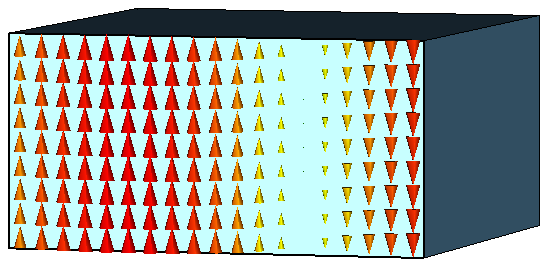
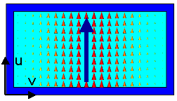
upPort ModesCST MICROWAVE STUDIO solvers generally allow using more than just the fundamental mode in the waveguide port. This becomes especially important when higher order modes need to be taken into account. In the pictures below, the first three modes of an empty waveguide are shown, sorted by their respective cutoff frequency. The number of propagating modes vary due to the chosen frequency range. As a rule, the number of modes to be considered at a waveguide port should at least be the number of propagating modes, because unconsidered modes will be reflected by the port operator.
If an evanescent port mode result is selected, a box will appear visualizing the distance from the port where the port mode has decayed by -40dB:
Multiple waveguide modes can convert energy into each other at the structure’s discontinuities. Due to these phenomena, the S-parameters of the propagating modes can also be affected by the evanescent modes. Therefore a certain number of evanescent modes needs to be taken into account. We recommend that the number of modes used for the simulation be chosen such that the -40dB distance of the last considered mode is shorter than the distance to the next discontinuity. This setting will ensure that all modes not considered for the simulation will make only very small contributions to the mode conversion. Mode PolarizationIn the case of quadratic or circular waveguides, the mode polarization is an issue. Please find a detailed discussion in the section Mode Polarization. upCoaxial WaveguidesThe most frequently used waveguide type of this category is the coaxial cable shown in the picture below:
upPort CreationThe port assignment for this type of waveguide is very simple. However, it is important to make sure that the port covers the entire cross-section of the coaxial cable. The easiest way to define the port face is to pick structure elements such as points / edges / faces before opening the port definition dialog box. The port dimensions will then automatically adjust to the bounding box of the picked elements. In most cases, the outer conductor part of the coaxial cable will be modeled with a solid cylinder. If this is the case, simply pick the end face of the conductor as shown below:
The bounding box of the picked end face will then define the dimension of the port. Note that the waveguide port is still shown as a rectangular face. However, the computation of the waveguide mode will be automatically restricted to the interior of the coaxial cable. If the end face of the outer conductor can not be picked for some reason, you can also pick edges or points on the circumference of the coaxial cable as described for the empty waveguides.
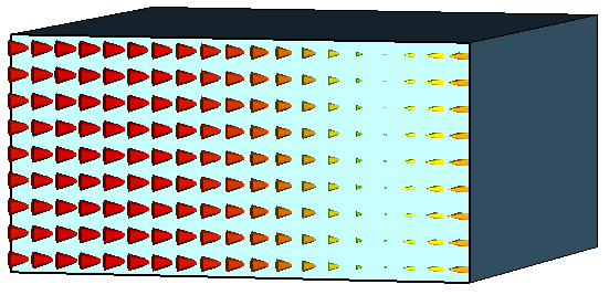
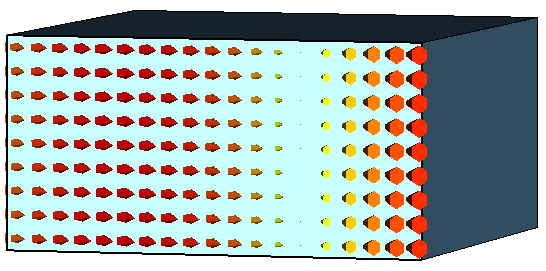
upPort ModesIn most cases, you will need to consider the fundamental mode of the coaxial cable so that you don’t need to worry about the number of modes for the port. The mode is automatically polarized so that the electric fields point from the inner conductor to the outer conductor as shown in the following picture:
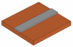
upMicrostrip LinesThe microstrip line is one of the most commonly used transmission lines for high frequency devices.
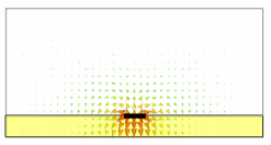
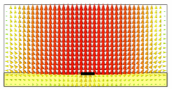
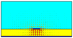
Unfortunately, this line type is relatively complex from an electromagnetic point of view. Therefore a few things need to be considered when defining ports for this type of structure. This type of structure requires modeling the air above the microstrip line, too. The easiest way to achieve this is to specify an extension in the Background Material dialog box. upPort Modes / Port DimensionsIn general, the size of the port is a very important consideration. On one hand, the port needs to be large enough to enclose the significant part of the microstrip line’s fundamental quasi-TEM mode. On the other hand, the port size should not be chosen unnecessarily large because this may cause higher order waveguide modes to propagate in the port. The following pictures show the fundamental microstrip line mode and higher order mode.
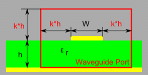
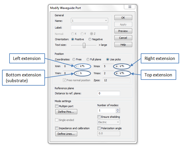
The higher order modes of the microstrip line are very similar to modes in rectangular waveguides. This behavior can be explained by an enclosure that is automatically added along the port’s circumference for the port mode calculation. The boundary conditions at the port’s edges will adopt the settings from the 3D model. In case of an ”open” boundary in the 3D model, a ”magnetic” port boundary will be used. This enclosure around the port causes the port to behave like a rectangular waveguide and thus is responsible for the particular pattern of the higher order modes. The larger the port, the lower the cut-off frequency of these modes. Since the higher order modes are somewhat artificial, they should not be considered in the simulation. Therefore, the port size should be chosen small enough that the higher order modes can not propagate, and only one (fundamental) mode should be chosen at the port. If higher order microstrip line modes become propagating, this normally results in very slow energy decays in the transient simulations and sharp spikes in the frequency domain simulation results, respectively. On the other hand, choosing a port size too small will cause degradation of the S-parameter’s accuracy or even instabilities of the transient solver. If you experience an unexpected behavior like this, check the size of the ports. As a rule, the size of the port is determined by the so-called extension factor k, according to the following picture:
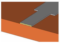
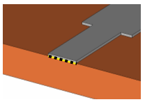
Its optimal value varies in a range from 5 to 10 depending on the ratio w/h, on the substrate permittivity and on the frequency range (because of frequency dispersion of the fundamental QTEM mode). The size of the port can be briefly verified by visualization of the E and/or H field of the port mode. If the field is obviously trimmed by the port border, its size should be enlarged and vice versa. A more reliable approach is to assess the k factor form the convergence curve of the line impedance, while k is swept in a reasonable range, e.g. 3 -15. upPort CreationOne way to define the port for this type of structure is to enter all its coordinates numerically. However, since this is a cumbersome solution, we will illustrate how ports for microstrip lines can be defined based on picked geometry. You can pick the entire end face of the microstrip line or pick the edge of the end face which is located on the surface of the dielectric substrate. The following pictures illustrate these options:
After picking the geometry, you can open the port
definition dialog box (Simulation:
Sources and Loads
Note: Make sure to enter exactly the height of the substrate for the port extension below the microstrip line or you will introduce some unwanted additional space between the substrate and the ground metallization, or the port may not be connected to ground at all. We therefore recommend defining a parameter for the substrate’s height (e.g. h). This parameter can then be used for specifying the bottom extension as shown above.
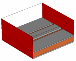
The explanations given above mainly refer to the unshielded microstrip lines. When a shielded microstrip problem needs to be simulated, the port can usually be chosen in such a way that it covers the entire dimension of the structure. The physical problem of unwanted box resonances appears much earlier in these cases than the artificial problem of unwanted propagating modes so that you do not need to worry about the latter here. The picture below shows the assignment of ports for a shielded structure with perfect electric conducting walls at each side:
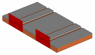
The easiest way to define a waveguide port covering the entire boundary face of the computation domain is to use the Full plane option in the port definition dialog box rather than using previously picked elements. Some structures require more than one microstrip line being located at the same boundary of the computation domain. If the microstrip lines are far enough away from each other the interaction of fields is negligible. Then ports can be assigned in the same way as described above using the same port size rule. An example for a structure like this is shown in the picture below:
If the lines get even closer, then they no longer work as two independent microstrip lines since the mode fields interact with each other and the waveguide becomes a multipin waveguide. Please refer to the Multipin Port Overview for this type of waveguide. Another important aspect in the simulation of microstrip lines is that the mode pattern is frequency dependent (unlike the mode patterns in empty guides or coaxial lines). The frequency domain solvers automatically recalculate the mode patterns for every frequency point so that this frequency dependent behavior does not cause a difficulty for the analysis. In contrast, the time domain solver uses the same mode pattern for the entire frequency band which may cause port mode mismatches at frequencies other than the mode calculation frequency. The error increases with increasing distance to the mode calculation frequency. By default, the transient solver computes the mode pattern at the center frequency of the frequency band, but this behavior can be changed by specifying the Mode calculation frequency in the solver specials dialog box on the Waveguide page. Despite this small mismatch at the ports, broadband simulation results will still be sufficiently accurate in most cases. However, very high accuracy requirements or very large bandwidths may require you to activate the inhomogeneous port accuracy enhancement option in the transient solver dialog. box. This feature will improve the accuracy of the S-parameters but on the other hand will slow down the simulation. upCoplanar LinesThe coplanar line is a frequently used transmission line for high frequency devices. Depending on whether the substrate is backed by a metallic shielding or not, the waveguide is either called ungrounded coplanar line or grounded coplanar line.
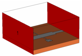
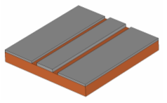
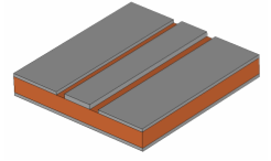
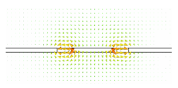
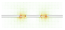
Unfortunately, this waveguide type is relatively complex from an electromagnetic point of view. Therefore some things need to be considered when defining ports for this type of structure. Many of the explanations in this subsection are similar to those for the Microstrip line case. However, we will repeat everything here once again for your convenience. upPort Modes / Port DimensionsFirst of all, the size of the port is a very important consideration. On one hand, the port needs to be large enough to enclose the significant part of the coplanar line field. On the other hand, the port size should not be unnecessarily large because this may cause higher order waveguide modes to propagate in the port. The following pictures show the fundamental even and odd modes as well as a higher order mode for an ungrounded coplanar waveguide:
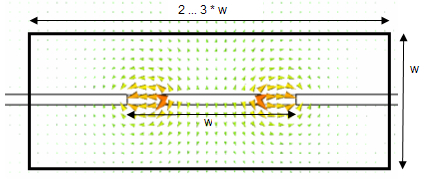
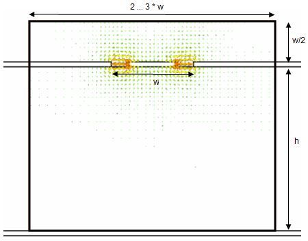
The higher order modes of the coplanar line are very similar to modes in rectangular waveguides. This behavior can be explained by an enclosure that is automatically added along the port’s circumference for the port mode calculation. The boundary conditions at the port’s edges adopt the settings from the 3D model. In case of an ”open” boundary in the 3D model, a ”magnetic” port boundary is used. This enclosure around the port causes the port to behave like a rectangular waveguide and thus is responsible for the particular pattern of the higher order modes. The larger the port, the lower the cut-off frequency of these modes. Since the higher order modes are somewhat artificial, they should not be considered in the simulation. Therefore, the port size should be chosen small enough that the higher order modes can not propagate, and only the fundamental modes should be considered at the port. If higher order coplanar line modes become propagating, this normally results in very slow energy decays in the transient simulations and sharp spikes in the frequency domain simulation results, respectively. On the other hand, choosing the port size too small will cause degradation of the S-parameter’s accuracy or even instabilities of the transient solver. If you experience an unexpected behavior like this, check the size of the ports. In the following we will draw a distinction between grounded and non-grounded coplanar lines. The following pictures show the recommended sizes of the port for both cases:
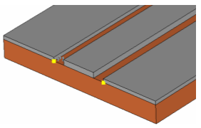
Ideally you would make the port three times as wide as the width of the inner conductor plus the width of the two gaps, but this may be reduced to around two times the inner conductor width plus the gaps in case of geometrical constraints. For ungrounded coplanar lines, you should enlarge the port by at least half of the inner conductor’s width plus the width of the gaps above and below the metallization. For grounded coplanar lines the same is true above the inner conductor, but you should make the port large enough to touch the ground metallization below. upPort CreationOne way to define the port for this type of structure is to enter all its coordinates numerically. However, since this is of course a very cumbersome solution, we will illustrate how ports for coplanar lines can be defined based on picked geometry. The easiest way to define a coplanar waveguide port is to pick the two innermost substrate corners of the outer conductors as shown in the picture below:
After picking the geometry, you can now open the
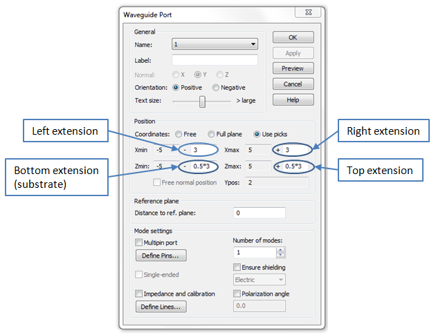
port definition dialog box ((Simulation:
Sources and Loads
You need an extension space of ideally the width of the inner conductor plus the gaps line (here 3) at each side of the inner conductor line. Furthermore, you should specify a distance of half of the width of the inner conductor plus the gaps above and below the inner conductor. In the case of grounded coplanar lines, make sure to enter exactly the height of the substrate for the port extension below the inner conductor or you might introduce some unwanted additional space between the substrate and the ground metallization, or the port may not be connected to ground at all.
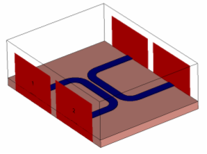
The explanations above mainly refer to unshielded coplanar lines. When a shielded coplanar line problem needs to be simulated, the port can be normally chosen so that it covers the entire dimension of the structure. The physical problem of unwanted box resonances appears much earlier in these cases than the artificial problem of unwanted propagating modes so that you do not need to worry about the latter here. The picture below shows the assignment of ports for a shielded structure with perfectly electric conducting walls at each side:
The easiest way to define waveguide ports covering the entire boundary face of the computation domain is to use the Full plane option in the port definition dialog box rather than using previously picked elements. Some structures require more than one coplanar line located at the same boundary of the computation domain. In general, you should try to avoid this situation if possible because it adds complexity to the port assignment. However, if the coplanar lines are far enough away from each other that the interaction of fields is negligible, ports can be assigned in the same way as described above using the same port size rule. An example for a structure like this is shown here:
If the lines get even closer, then they no longer work as two independent coplanar lines since the mode fields interact with each other and the waveguide becomes a multipin waveguide. Please refer to the Multipin Port Overview for this type of waveguide. If no symmetry condition is defined in the middle of the coplanar line, both even and odd modes can exist and therefore need to be taken into account. If an electric symmetry condition is specified, only the odd mode can exist. On the other hand, setting a magnetic symmetry condition will consider the even mode only. If the microstrip line is grounded, another parasitic microstrip mode will exist too as long as no electric symmetry is defined. All this leads us to the following table for the number of modes normally used for the simulation at the coplanar port:
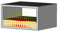
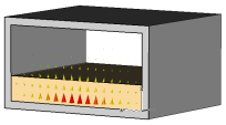
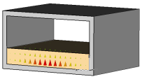
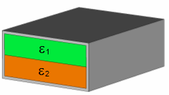
The corresponding number can be specified in the Number of modes field in the port properties dialog box. Note that the order in which the port modes are calculated may vary depending on the dimensions of the structure as well as the frequency. Therefore we highly recommend always inspecting the port mode results in order to avoid misinterpreting the S-parameter data. Another important aspect in the simulation of coplanar lines is the fact that the mode pattern is frequency dependent (unlike the mode patterns in empty guides or coaxial lines). The frequency domain solvers automatically recalculate the mode patterns for every frequency point so that this frequency dependency does not constitute a difficulty for analysis. In contrast, the time domain solver uses the same mode pattern for the entire frequency band which may cause port mode mismatches at frequencies other than the mode calculation frequency. The error increases with increasing distance to the mode calculation frequency. By default, the transient solver computes the mode pattern at the center frequency of the frequency band, but this behavior can be changed by specifying the Mode calculation frequency in the solver specials dialog box on the Waveguide page. Despite this small mismatch at the ports, the broadband simulation results are still sufficiently accurate in most cases. However, very high accuracy requirements or very large bandwidths may require you to activate the inhomogeneous port accuracy enhancement option in the transient solver dialog. box. This feature will improve the accuracy of the S-parameters but on the other hand will also slow down the simulation. upInhomogeneous Waveguide Ports (Special Treatment)A waveguide is called inhomogeneous whenever more than one different dielectric material is present in the cross-section of the waveguide. As mentioned before this is the case for microstrip lines and coplanar lines as well as for dielectrically loaded waveguides, representing QTEM and no QTEM modes respectively. The most important fact of inhomogeneous waveguide ports is that the mode pattern is frequency dependent. As an example in the pictures below the basic TE mode of a dielectrically loaded waveguide is presented for three different frequency points. The higher the frequency (from left to right), the more the field is concentrated in the material with the higher dielectric value (colored in light brown).
The frequency domain solvers automatically recalculate the mode patterns for every frequency point so that this frequency dependent behavior does not cause a difficulty for the analysis. In contrast, the time domain solver uses the same mode pattern for the entire frequency band which may cause port mode mismatches at frequencies other than the mode calculation frequency. The error increases with increasing distance to the mode calculation frequency. By default, the transient solver computes the mode pattern at the center frequency of the frequency band, but this behavior can be changed by specifying the Mode calculation frequency in the solver specials dialog box on the Waveguide page. Despite this small mismatch at the ports, broadband simulation results will still be sufficiently accurate in most cases. However, possibilities to achieve very high accuracy requirements or very large bandwidths are discussed in the following for microstrip lines / coplanar lines (QTEM Modes) and dielectrically loaded waveguides (No QTEM Modes). upMicrostrip Lines / Coplanar Lines (QTEM Modes)Because of the inhomogeneous port region, the waveguide port operator works less accurately with increasing distance from the mode calculation frequency. However, the occurring broadband error may be prevented and the accuracy of the S-parameters improved with help of the inhomogeneous port accuracy enhancement feature, achievable in the transient solver dialog. This feature requires the excitation of all port modes and thus will slow down the simulation - it is therefore advisable to activate this functionality carefully and if possible together with the usage of S-parameter symmetries. Dielectric losses in the port region can not be directly considered during the time domain calculation. However, using this feature, it is possible to consider their influence in a post processing step.
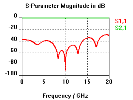
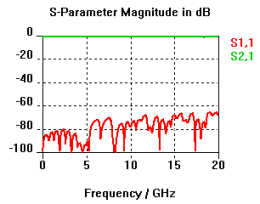
A single microstrip line is calculated with two normal waveguide ports as demonstrated in the following picture:
Due to the chosen mode calculation frequency, the reflection is accurate only in the range about 10 GHz. In contrast to this, the right picture shows the result of the calculation applying the inhomogeneous port accuracy enhancement. Here, the reflection is less than &endash;60 dB over the complete frequency range as to be expected.
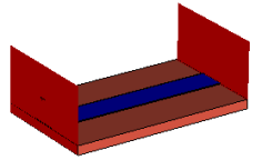
upDielectrically Loaded Waveguides (No QTEM Modes)The following explanations therefore exclude these types of waveguides and focus on dielectrically loaded waveguides. A typical example is shown in the following picture:
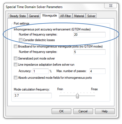
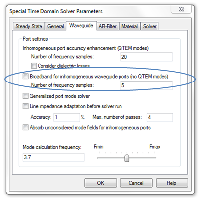
In terms of assigning ports to these waveguides, the procedure is very similar to the Empty waveguide case explained earlier in this section. The main difference here is that the port mode pattern is no longer frequency independent. The frequency domain solvers automatically recalculate the mode patterns for every frequency point so that this frequency dependency does not constitute a difficulty for the analysis. In contrast, the time domain solver uses the same mode pattern for the entire frequency band which may cause port mode mismatches at frequencies other than the mode calculation frequency. The error increases with increasing distance to the mode calculation frequency. If you are interested in only very small frequency ranges, a viable solution may be to set the mode calculation frequency equal to the center frequency of this frequency band. This setting can be made by specifying the Mode calculation frequency in the solver specials dialog box on the Waveguide page. However, if you are interested in broadband results within larger frequency ranges, the transient solver needs to be advised to make a special (and computationally expensive) treatment for the inhomogeneous ports. The Broadband for inhomogeneous waveguide ports (no QTEM modes) option can also be activated on the Waveguide page of the solver’s specials dialog box:
This option will provide much more accurate broadband results for this type of port. Unfortunately, it is limited to the fundamental (propagating) mode only. upGeneralized port mode solverThe generalized port mode solver can be used for any kind of homogeneous or inhomogeneous waveguides.
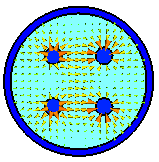
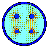
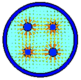
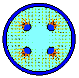
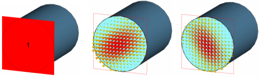
It will analyze the broadband behavior of the specified modes in a preprocessing step. Afterwards this behavior is considered in the time domain calculation, so that accurate broadband results can be obtained. Please note that this can cause higher numerical effort compared to the normal waveguide port solver. There is no restriction on the type of mode, even hybrid modes can be considered. Multipin Waveguide PortsA multiple conductor or multipin waveguide port is characterized by having more than two conductors (e.g. two inner conductors plus shielding) in the port. According to this definition, a coplanar line is also a multipin waveguide. However, due to the importance of this particular transmission line type, it is explained in detail in a subsection above. Due to their complexity other types of multipin ports are only briefly mentioned in the following subsections and are discussed in detail on a separate page, the Multipin Port Overview. Homogeneous Multipin PortsIn case of a homogeneous multipin port the occurring TEM modes are degenerated (having the same propagating constant) and can be superposed to new mode patterns because they are orthogonal to each other. As an example the following coaxial multipin port consists of one outer and four inner conductors, such that four different TEM modes exist:
Consequently, the mode patterns shown here represent just one possible solution. Therefore it is advisable to specify the mode pattern that you want to excite by using the multipin operator functionality that enables the combination of the static modes according to your wishes. Please see the Multipin Port Overview page for more details about this kind of port operator.
upInhomogeneous Multipin PortsIn case of slightly inhomogeneous coaxial waveguide or connector ports, it might still by suitable to superpose the resulting QTEM modes by use of a Multipin Port as mentioned in the previous section. However, please keep in mind that the propagation constants differ between the modes; this will lead to some inaccuracies, depending on the inhomogeneity of the port. In case that the inhomogeneity error is not negligible anymore all ports should be defined as single-ended. After the simulation is finished the single-ended S-parameters are calculated as a postprocessing step and can then be recombined in CST DESIGN STUDIO by differential excitations resembling the multipin configuration of the structure. Please find more information about single-ended S-Parameter calculation on the Multipin Port Overview page. The same holds also in the special case of inhomogeneous microstrip ports with multiple conductors as shown below:
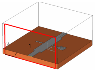
Here the coupling effects between the single conductors can also be analyzed by means of single-ended ports. upPeriodic Waveguide PortsFor the hexahedral Frequency Domain Solver, it is possible to consider periodic port boundaries with a nonzero phase shift. These boundary characteristics correspond to the global settings made in the Boundary Condition dialog. See below an example of a simple waveguide structure with one periodic boundary.
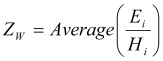
upGeneral InformationLosses in Waveguide PortsIf a waveguide port contains losses, either in the form of a lossy dielectric substrate or due to lossy metal, some restrictions appear for specific solvers; these restrictions are discussed in the following. Currently, for the Transient Solver losses can be considered for QTEM modes using the inhomogeneous port accuracy enhancement feature. Please activate the consideration of dielectric losses in the special waveguide port settings for this purpose. If not activated, slight unphysical reflections caused by losses in the port region possibly overlay the broadband error produced by inhomogeneous material. If activated, the influence of the reflections on the S-Parameters can be deembedded by taking complex propagation constants into account. Please note that the surface impedance model for lossy metal is not supported. The Frequency Domain Solvers (except the resonant solvers) consider lossy materials in ports and calculate complex propagation constants. Also note that the Frequency Domain Solver with hexahedral mesh does not support the surface impedance model for lossy metal. upImpedance DefinitionWave impedanceFor all types of waveguide ports, the value of the wave impedance is calculated, correspondent to the average ratio of the transversal electric field to the transversal magnetic field for all grid points [ i ] in the port plane:
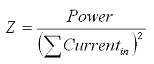
However, to avoid errors from division of small numbers, the field values below a certain level (referred to the maximum field value) are not included in this calculation. Z-Wave-SigmaThe standard deviation of the averaged wave impedance calculation as described above can be found in the solver logfile as Z-Wave-Sigma. Line ImpedanceFurthermore, in case of an arbitrary multiple-conductor port (coaxial waveguide port, microstrip line, connector port, etc.), where static mode patterns (TEM or QTEM modes) exist, the value of the line impedance is calculated. This is performed for each mode separately by considering all conductor currents heading into the structure using the following expression:
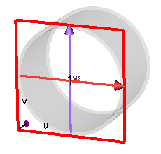
Here, the power is given as the integral of the Poynting vector over the port area and the currents are calculated by integrating the magnetic field in a small distance around the conductors’ surfaces. Note: Please be aware that this formulation differs from the commonly used definition Z = U / I and thus may lead to different results. Please find a demonstration on the Multipin Port Overview page. upMode CalibrationTo receive a consistent orientation of the calculated mode pattern, the electric mode field is calibrated due to some specific rules; the magnetic field is then determined by the power flow of the excited port. This means that the Poynting vector of the mode pattern always points in the direction of the port radiation. With this, it is possible to connect ports of various structures in CST DESIGN STUDIO without producing unwanted phase shifts. The pictures below show the calibration of port modes with respect to the orientation of the electric field. In an empty waveguide, the electric field components are orientated with respect to the local u/v-coordinate system of the port. If an inner conductor is found (for ports with two or three conductors), the divergence calculation of this conductor pin will be positive, i.e., the electric field is directed to ground, as can be seen in both pictures on the right (a microstrip line and a coaxial waveguide). All other port modes are orientated corresponding to the port's coordinate system similar to the empty waveguide port. However, in any case the consistency for a port coupling in CST DESIGN STUDIO is ensured. Multipin port modes use the potential pin definition to determine the orientation of the electric field components, please refer to the Multipin Port Overview page for more information.
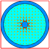
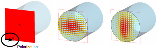
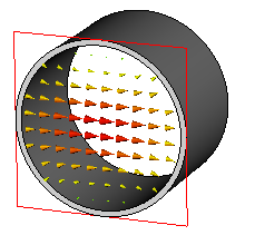
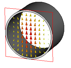
Calibration linesAs mentioned above, the calibration of modes is performed automatically in the entire port region. However, for models with tetrahedral mesh representation, calibration lines may be used to limit the mode calibration to a given line instead of using the entire port region. This is useful if a inhomogeneous material is used in the port region resulting in large electric fields at locations different from the calibration line. upMode PolarizationWhen mode degeneration occurs, two modes sharing one propagation constant may be linearly combined. There are two possibilities to define the polarization of degenerated modes, depending on the used mesh representation. Especially in the case of quadratic or circular waveguides, the mode polarization is an issue. For the example below, two propagating modes are calculated. By default, the orientation of these modes is arbitrary:
Note that the waveguide port is still shown as a rectangular face. However, the computation of the waveguide mode is automatically restricted to the interior of the waveguide. The most important point here again is that the port’s face covers the entire cross-section of the waveguide. Hexahedral MeshFor hexahedral mesh representations, a Polarization angle between 0 and 360 degrees can be defined in the waveguide port dialog. This angle refers to the main direction of the E&endash;fields for the first of the degenerated modes. This orientation of the fundamental mode’s electric field is then visualized by an arrow in the port face which is shown when the corresponding port is selected. The second mode will then be calculated perpendicularly to the first one:
Tetrahedral meshFor models using tetrahedral mesh, representation the polarization for degenerated modes can be defined using the Mode Impedance and Calibration dialog. Therefore, two polarization lines are needed to align the main directions of the E-Fields of two degenerated modes perpendicular to each other.
upEnsure shieldingEspecially for inner waveguide ports is important to apply an electric or magnetic shielding to ensure a consistent integration of the waveguide boundary into the calculation domain. In case of a hexahedral mesh, port shieldings are modeled as a tube in direction of field imprint, with a length of two grid cells. For tetrahedral meshes this extrusion is not necessary. Please not that the boundary condition can be influenced by a port shielding. Also, conductors might be short-circuited by an electric shield. Generally, a electric boundary condition or PEC material is given higher priority compared to a magnetic shielding. Furthermore, the solver detects whether the port contains an outer region (as in the corners of a coaxial line). If this is the case, shielding the port will not have any effect and is therefore not applied.
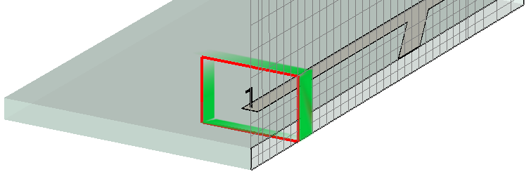
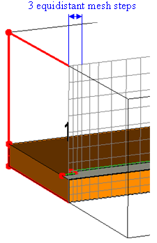
Fig.: Schematic view of an electric shielding applied to an inner waveguide port. upWaveguide Ports in Hexahedral Mesh ViewBefore starting a simulation, every structure must be spatially discretized. The same holds for a waveguide port. For consistency reasons, the same mesh is used for the port as for the structure. Therefore, it might become clear that the dimensions of the port definition must not necessarily be the same as those used for the simulation. The dimensions must be mapped onto the mesh and therefore might change slightly. However, the port dimensions will always be enlarged; they will never shrink. To control how the dimensions are observed by the simulation, you may enter the mesh mode. There, the mapped ports are plotted with a red frame.
upSee alsoExcitation Source Overview, Waveguide Port, Multipin Port Overview, Broadband Ports, Discrete Port Overview, Time Signal View, Reference Value and Normalization
HFSS视频教程 ADS视频教程 CST视频教程 Ansoft Designer 中文教程 |
||||||||||||||||||||||||||||||||||||||||||||||||||||||||||||||||||||||||||||||||||
|
Copyright © 2006 - 2013 微波EDA网, All Rights Reserved 业务联系:mweda@163.com |
|