
The EDA Import Dialog
is opened automatically when creating 3D simulation models from PCB/package
layouts, or when using the functionality "Export to MWS..."
from within CST PCB STUDIO.
The present dialog allows the user to perform the following tasks:
The following fields appear in the dialog:
Files
Shows the file path of the PCB database being processed.
Log File tab
Prints progress information.
Cancel
Cancels open procedure.
OK
Returns to the main application and creates the 3D model of the PCB.
The following parameters influence the setup of the 3D model:
For viewing / modifying the layer stack-up table.
Background: EDA CAD tools normally provide layer-thicknesses data as 'effective', i.e. real layer thicknesses after manufacturing. Thus, the thickness of a substrate layer specifies the distance between attached copper layers in the physical PCB. As an effect of the manufacturing process, copper layers are somehow pressed into adjacent soft substrates (so-called Prepregs) whereas they are just glued on top of hard substrates (so-called Cores). It is the task of the PCB manufacturers to account for these effects by choosing the right raw substrates. In this way, the physical PCB will have the same dimensions as those given the CAD layer stack-up, as shown in the following picture (4-layer PCB by foil construction, solder mask neglected):
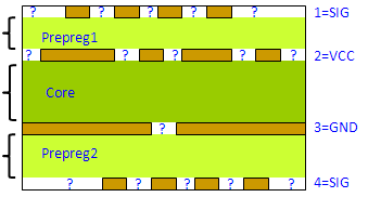
As can be seen, the filling of voids in the copper layers (which happens through flow processes from adjacent substrates during manufacturing) is not fixed by the given data. For that reason, these additional pieces of information can be supplied in the present dialog (see field 'Filling from' below). Naturally, the nature of substrates (Core/Prepreg) determines how the void filling happens: 1-from below, 2-from above, 3-from below, 4-from above:
In order to offer maximum flexibility, the substrate thicknesses can also be handled as 'raw', meaning that the effect of pressing in copper layers is considered explicitly here: The copper layers are pressed into substrates as specified in the 'Filling from' field, but the copper thicknesses do not contribute to the overall PCB thickness.
The columns of the table have the following meaning:
Name
Name of the given layer. Not editable.
Material
Name of layer material. Not editable. By right-clicking and selecting "Duplicate material" in the drop-down menu, the layer material becomes independent from those of other layers.
Cond. / tan delta
For "lossy metal"-type layer, specifies the electrical conductivity in Siemens/m, for "dielectric" layers, specifies the loss angle (d) through tan(d). If the value of tan(d) is nonzero, the material model used in CST MICROWAVE STUDIO® will be a first-order Debye model (Material Overview), which also requires the definition of the measurement frequency of the specified permittivity and tan(d). This frequency can be also specified in the present column using the syntax "0.02@1.5GHz", which means that the permittivity and tan(d)=0.02 are found at 1.5GHz. Please note that a zero frequency specified here will be replaced by the center of the frequency window defined in CST MICROWAVE STUDIO®.
Permittivity
Relative electrical permittivity of the layer material.
Thickness
Layer thickness in the length unit of the stack-up table, see below.
Elevation
Elevation of the layer above z=0. The column automatically updates itself when the user changes layer thicknesses.
Filling from
This switch controls how the voids of copper layers are filled by adjacent substrate material. Options:
"Above": the substrate above the copper layer is supposed to fill the voids
"Below: the substrate below the copper layer is supposed to fill the voids
"Both": voids are filled by both substrate materials by an equal amount
Effective Thicknesses
When switched on the stack-up data is considered as 'effective', as opposed to 'raw', see the above background for an explanation of these terms.
The Unit switch
lets you choose the length unit for layer thickness and elevation in the stack-up table (micrometers or mils).
Load...
Load the stack-up table from a file.
Save...
Save the stack-up table to a file.
For viewing / modifying the parameters associated with components and parts.
Background: For the purpose of signal/power integrity simulations, a part is characterized by the following pieces of information: part number, pin list, and electromagnetic model. The former two are fixed within the design, whereas the latter can be customized by the user. Currently, only two-pin, passive parts are supported by the EDA import, corresponding to the Lumped Element model. For the case of resistors, inductors, or capacitors, the corresponding R, L, and C values are extracted from the PCB database, if present. Components, on the other hand, describe the placement of part items on the board (position, rotation, mount type, layer). They are addressed by their so-called reference designator (e.g. "R101", "L392", "C901").
Refdes
A list of all reference designators contained in the database.
Part
The currently assigned part to the component. By right-clicking the part name, a context menu appears that allows to change or unset the current part assignment. Choosing change (or double-clicking) will launch the Part Library, from which a part can be chosen by selecting a part and clicking "OK". A third option called "Create missing RLC-part" is available when there are parts specified, that are not defined in the current part library. Choosing this option results in the creation of an RLC-part with invalid values, which the user needs to set manually.
Info
A descriptive information text about the electromagnetic model pertaining to the part.
Load...
Load part EM model data (currently, only 2-pin RLC values) from a file.
Comma-separated values file (*.csv)
This is a plain text file, readable e.g. by Microsoft Excel. The .csv file should exhibit at least three columns with headers "refdes", "partname", and "value", separated by comma, semicolon, colon or tab character. Column "refdes" contains the component references (e.g. "R101"), column "partname" denotes the part IDs (manufacturer ID or enterprise-wide part ID), whereas the column "value" contains the lumped-element values (units are Ohms, nano-Henries, and pico-Farads). For correct interpretation of values, the respective types of components (R, L, or C) must be known. This type can be specified in an additional column, "type", containing one of 'R', 'L', or 'C'. If the "type" column is absent, the first character of the "refdes" will be used as type specifier.
Note: when using Microsoft Excel to view the .csv file, consider using the "Filter" option for easy sorting and filtering the table.
Cadence components file (*.txt)
From Cadence Allegro PCB Editor, this text file can be produced by the report mechanism. In Cadence Allegro, please type "old_reports" in the command window. In the dialog box appears, select "Components" and specify the output filename (e.g. components.txt). Pressing "Report" will produce the file that can be loaded into the part editor.
Part Library...
This will open a new window providing access to the Part Library. The part library allows the user to build up a library of parts, which can be stored and loaded. Currently only 2-pin RLC parts are supported.
Part
The name of the part. Not editable.
Info
A descriptive information text about the electromagnetic model pertaining to the part.
Editor
To the right of the table, the embedded editor allows the user to change the values for a selected part.
Load...
Ability to load a all parts from a previously stored CST Part Database library file (.dat). If conflicting part names exist, these part names can replaced, skipped or added uniquely to the existing database.
Save...
Saves the current Part Library to a CST Part Database file (.dat).
New Part...
Opens up a new window in which the user can specify a part name, and set its RLC values.
Remove Part
Removes the currently selected part from the current database.
Import components
If turned on (default) then the components get imported into CST MICROWAVE STUDIO.
A preview of the PCB is displayed in this tab, with the intent that the user may graphically select a subset of the total board. For highly complex designs, treating the board as a whole may not be desirable due to simulation performance so that a selection procedure becomes mandatory.
Layer shapes can be displayed or hidden using this check-box matrix. The rows of the matrix correspond to the conductor layers (layer name in the first column), where "*" means "all layers". The meaning of the columns if as follows:
"*" Toggle visibility of all shape types
 wire-frame/filled
display for plane shapes and pads
wire-frame/filled
display for plane shapes and pads
 display
traces (always displayed as thin lines)
display
traces (always displayed as thin lines)
 display
plane shapes
display
plane shapes
 display
pad shapes
display
pad shapes
 display
component outlines
display
component outlines
 display
selection polygons
display
selection polygons
 display
generated etch shapes
display
generated etch shapes
Net Highlighting
Nets can be highlighted by selecting them, and net types ("sig", "pwr", "gnd") can be changed for one or multiple nets at a time. Columns "Sel.", "Name", and "Type" hold the selection state, name, and net type, respectively, for each net.
Please use the filtering option for restricting the list to the interesting nets.
Restrict to selected...
Within this group of tools, the geometry to be imported into the 3D model can be restricted, in order to reduce simulation complexity (see example below).
Area
Use this option to restrict the 3D model to the copper geometries contained within a defined area.
If checked, a selection rectangle or polygon may be drawn in the board view: right-click in the view window and select "New rectangular/polygonal selection". For rectangular selection, just left-click at one corner, draw the rectangle, then release the mouse button. For polygonal selection, left-click at the starting position of the polygon and add further points by additional left-clicks. In order to close the polygon, right-click and choose "Done" from the pop-up menu. When the grid option is turned on, all selected points will be snapped to the grid during the selection procedure (a polygon may now also be closed by clicking on the start position). Holding down the Shift-key will allow for purely horizontal, vertical and 45-degree selection.
Alternatively, a restriction area can be auto-generated around selected signal nets (traces), where the area contains all points within a given distance to the traces: When pushing the "Area" button, a pop-up dialog will query the user for this inclusion distance ("Include shapes within distance"). The option "Consider power/ground nets" allows to include/exclude the supply nets into the area computation.
After the selection area has been defined, a dialog will pop-up in which the user can specify for which layers the selection should be effective. Multiple selection areas may be defined for each layer and the selection areas may overlap. Clicking on a point belonging to an already defined polygon, will make the selection active. Right-clicking will bring up a pop-menu with the following options:
Remove point on polygon: Removes the selected point from the polygon.
Change layer selection: Brings up the layer selection dialog to modify previous selections.
Snap shape to grid: (re)snaps the selected polygon to the currently defined grid.
Delete selected polygon: removes the selected polygon.
Delete all polygons: deletes all selection polygons on all layers.
When creating the etch shapes from the traces, planes, and pad shapes, all geometries will be clipped to the selection area.
Nets
If checked, only shapes belonging to the selected electrical nets will be considered for import.
Layers
If checked, only selected layers will be considered for import. Pushing the button opens a layer-selection dialog.
Example (cross-talk between two signal nets): Select the coupled nets in the "Net Highlighting" window. Then, create a selection area around the two nets using the "Area" functionality. Now, if needed, also select reference nets (e.g. GND, VCC) and enable "Restrict to selected nets". The resulting 3D model will comprise the two signal nets and their reference planes, restricted to the selection area.
Manually defining many discrete ports in the 3D model may be time-consuming. Alternatively, discrete ports can be defined already in the EDA Import Dialog: By using the logical information contained in the layout (pins, nets), the present dialog offers a convenient means for generation the desired external connections needed for the simulation. In addition to the integer number of the ports, port labels are generated in the 3D model in order to identify the pin(s) a port is attached to.
In the dialog, the left-hand-side list displays all pins in the layout, including the respective component and net. This table can be sorted by each column, thus allowing to easily find all pins of a given net, for instance. The filtering option supports the navigation in the pin list.
(i) Differential ports
As every pin corresponds to a predefined 3D position (normally on the surface of the layout), ports can be defined by connecting pairs of pins. Only pairs of pins of the same component are sensible to consider here. If N pins of a certain component are to be excited in the simulation, N-1 differential ports are needed to completely characterize the situation. These N-1 ports form a spanning tree between the selected pins, see the following picture. If only a subset of all pins of the component are selected, it is easy to imagine that the horizontal wires forming the ports may intersect the pin-pads of unselected pins, thus leading to shorts. In order to prevent producing shorts, vertical wire leads are automatically added on top of the selected pins, see figure. The height of leads can be manipulated in the separate dialog Specials...->Ports / Lumped elements
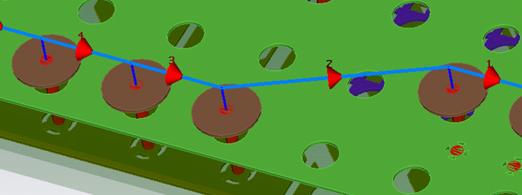
Figure: Automatically generated differential ports
For generating differential ports, one selects a set of pins in the pin list and presses the arrow button pointing to the "differential ports" group on the right. The dialog will automatically construct the spanning tree(s) for each of the involved components. Ports can be deleted by selection and pressing the "delete" key. In the layout view, the ports will appear as blue arrows between pins.
Note: The port impedance will be set to 100 Ohms.
(ii) Single-ended ports
As a second option for port generation, every selected pin can be connected to a close-by reference conductor (net or PEC sheet, see Specials...->Ports / Lumped elements).
For generating single-ended ports, please select pins in the pin list an click the arrow button pointing to the "single-ended ports" group on the right. Ports can be deleted by selection and pressing the "delete" key. Please note that, as a second step, it is mandatory to define the reference nets for each single-ended port. Using multi-selection, the same reference net(s) can be assigned to all selected ports.
Note: In the presence of a common reference net for all pins, the differential and single-ended approaches are equivalent, as voltage differences between two pins can either be expressed through the voltage difference between the associated single-ended ports, or through the sum differential ports that connect the two pins within the spanning tree. If no reference conductor can be identified, or its physical meaning is questionable, using differential ports is recommended, since this approach correctly reflects the voltage differences seen by the external component.
Note: The port impedance will be set to 50 Ohms.
Ports (geometrical definition)
In addition to the pin-based port definition, one can also define the start and end positions of a port graphically within the layout view. Here, we differentiate between two types of discrete ports:
vertically-oriented port (directed along z axis): By right-clicking in the layout view window, and choosing "Add vertical discrete port here...", a vertical port can be defined at the position of the mouse right click.
port with general orientation: By right-clicking in the view window, and choosing "Add general discrete port from here...", a discrete port with arbitrary start and end points can be defined, where the start point is given by the position of the mouse right click. The end point is defined by the next left-click.
After that, a dialog box appears that displays the current port number and two identical lists of the conductor layer names. The start layer (first list) and end layer of the port (second list) can be selected here (they have to differ in the vertical case). Clicking "OK" finishes the port definition. The lower tip of a blue triangle now indicates the location of the port.
Preview
For each layer selected for import, unite all conductor shapes (traces, plane shapes, and pads), if desired, restricted to the selected area and/or nets. The generated etch shapes correspond to the physical copper shapes and do not differentiate between the original shape types. However, net information is kept in etch shapes. The result is the set of shapes that will appear in the 3D model. In the layout view, these shapes can be displayed by activating the column "E" in the Layer Visibility matrix.
Check
Pressing this button runs a check of pin connectivity. Please note that a component pin is defined as a 3D point having a name and a net. If the PCB connectivity is correct, exactly all pins of the same net are connected (thus forming a group). The result of the pin-connectivity check is displayed in the spreadsheet, "Result of Connectivity Check": Columns "Refdes", "Pin", and "Net" denote the respective component name, pin name, and net. Column "Group" displays the number of the connectivity group the pin belongs to. Please note that this number is an arbitrary identifier for each group. Column "Remark" contains information of errors in connectivity, with the cases:
"isolated pin"
Indicates that there is no conductor at the pin position.
"net separated"
The pin is not connected to all other pins of the same net.
"connected to other nets"
The pin is connected to pins of other nets.
Parameters referring to length scales of copper shapes may be edited/inspected in this dialog.
As 2D sheets
If checked, PCB etch shapes will be represented as 2D sheets instead of 3D solids.
As 3D bodies
If checked, PCB etch shapes will be represented 3D solids of small, but non-zero thickness.
Tolerance
Determines the smallest relevant length of shape segments. Smaller segments will be eliminated upon cleaning, thus smoothing the respective etch shape (see background below). This length can also be considered as the supposed etch (xy) manufacturing tolerance. Default value is one micron.
Use straight-line geometry
When checked, the etching process will make use of an alternative, purely straight-line geometry kernel with high robustness. In this case, arced polygons will be approximated by straight-line segments. (Background: The default 2D geometry kernel performs computations on polygons consisting of straight lines and circular arcs. For some problematic input data, the arced parts may cause numerical instabilities, leading to the failure of the etching process on some layers. In this case it is recommended to switch on the present option.)
Suppress unconnected pads
If checked, unconnected (sometimes termed "unused") pads will be excluded from etch creation (and thus from the 3D model). It is possibly to choose between the following algorithms:
Valor
A pad is unconnected if it does not touch any other etch shape lying on the same layer. An unconnected pad is suppressed if it is not on the start or end layer of a drill (no matter if through-hole or blind/buried via).
PADS
Remove unused pads on Split/Mixed Planes (mainly for Mentor Graphics PADS Import). A pad is unconnected if it does not touch any other etch shape or touch shape from different net lying on the same layer. All pads on top and bottom layers remain unchanged.
PADS (keep start/end)
Like PADS, but preserve via pads on start and end layers.
Notes: If the flag for "Remove unused pads" is already activated in the PADS ASCII-File, the PCB-Import Dialog will get this information and use the appropriate algorithm.
Background: An essential feature of the CST EDA import is the automatic cleaning and healing procedure performed upon setting up the 3D model. In that way, the shape complexity of the model is reduced, leading to better performance of 3D electromagnetic simulations. By modifying the parameters discussed here, the user may directly take influence on the cleaning and healing algorithm.
Specials![]() Substrate layers
Substrate layers
Use axis-aligned bounding box of selection area
If checked (in the case that only a part of a PCB is imported using area selection), the substrate layers will be forced to be of axis-aligned, rectangular shape, irrespectively of the shape of the section area. The resulting rectangle will be minimum, but containing the selection area (also see the next option).
Extend area selection by
If the 'axis-aligned rectangles' option is checked, the rectangular substrate layers will be extended laterally by the distance specified here. Extending the substrate layers by a small amount using the present option can facilitate the mesh generation process for tetrahedral meshes.
Specials![]() Drills
Drills
Representation
Choice of drill-hole representation (round or segmented).
Increase via radii with drill-hole plating thickness
Many layout designs consider vias as finished holes, i.e. as drilled holes that were plated. Therefore, the finished holes have a radius equal to the drilled holes, decreased by the plating thickness. In principle these vias are hollow tubes. In MWS, these vias are represented as solid cylinders with the diameter of the finished hole. If checked, the user has the ability to slightly increase the via radii by the plating thickness in um, such that the via radii become equal to the drill-hole radii.
Deduce missing diameters
Sometimes, layout designs carry the convention that drill-hole diameters need not be specified explicitly, but can be taken from the set of pads that belong to the same padstack as the drill-hole. When checking this option, drills of diameter zero will be corrected to the smallest pad diameter contained within the padstack.
Specials![]() Bondwires (packages only)
Bondwires (packages only)
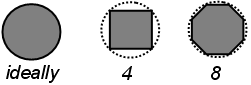
Number of segments for cross-sections
In order to keep the model complexity low, bondwire cross sections are always approximated by a chain of straight segments, see the following figure. The present field determines their number.
Separation factor for coincident bondwires
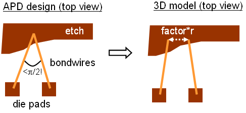
If two bondwires meet at a point (s. left figure below), the local geometric complexity of the 3D model will increase, as more surface shapes are needed to correctly model the junction. This can be avoided by slightly separating the bondwires' end points. The present factor determines the distance of this separation in terms of the mean radius of the two bondwires. The result in the 3D model is shown in the right picture below. (This modification is restricted to angles<p/2 between bondwires).
Minimum incidence angle to substrate
Given in degrees. See "Flat-incidence lift factor".
Maximum footprint on substrate
Given as an absolute length. See "Flat-incidence lift factor".
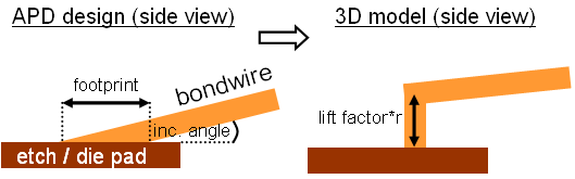
Flat-incidence lift factor
Flat incidence of bondwires causes a large footprint on the substrate, as shown in the left picture below. In the worst case, shorts between neighboring bondwires may occur, invalidating the 3D model. In order to avoid the problem, a small vertical segment is added, so that the bondwire footprint becomes minimum (see right figure). The vertical segment will be added if either the incidence angle is smaller than the given mininum or the footprint is larger than the specified, absolute length. The length of the segment will be the lift factor times the radius of the bondwire.
Specials![]() BGA/Bumps (packages only)
BGA/Bumps (packages only)
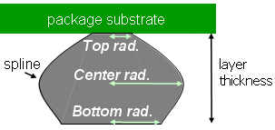
Solder ball radii[um]
This table allows for the adjustment of the top, center and bottom radius for all bump and BGA solder balls in the design, see picture below. Please note that the solder-ball geometry will in general be a rotated spline. If all radii are identical, solder balls will be modeled as cylinders. All sizes are given in micrometers (um).
Specials![]() Ports / Lumped elements
Ports / Lumped elements
Component elevation
This option defines the distance of component pins to the respective mounting layer. When unchecked, discrete ports and lumped elements will connect pins directly on the surface of top/bottom conductor layers, thus potentially leading to shorts in the presence of a third net passing in between the pins. When checked, discrete ports and lumped elements will be attached to the component pins by additional, vertical leads.
Up to solder mask
Using this option, vertical leads go from the conductor layer to the outer elevation of the attached solder mask.
Explicit height
Using this option, vertical leads are created vertically with an explicit user-defined length.
Single-ended port geometry
Edge to closest reference conductor
The search for the
reference point is carried out in the 3D geometry in order to make sure
that the connections are valid, see the next figure. An important requirement
for port validity is that the port edge does not intersect or touch other
conductors. This is checked within a geometrical tolerance given by the
parameter Specials...![]() Mesh
Mesh![]() lateral reference length (see below).
The respective search algorithm may shift the pin position to the boundary
of the pad if adequate.
lateral reference length (see below).
The respective search algorithm may shift the pin position to the boundary
of the pad if adequate.
Max. port length
This parameter specifies the maximum length of this kind of single-ended ports and has been introduced to prevent long computation times in case of failing reference-conductor search.
Prefer vertical orientation
When checked, ports are preferred that are approximately vertical.
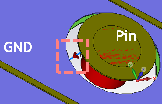
Figure: Automatically generated single-ended port
Edge to component PEC sheet
This option will introduce PEC sheets for all components for which ports have been specified. PEC sheets are perfectly-conducting sheets of about the size of the component footprint, that are always placed directly above or below the component's pins. Ports (and shorting wires) are then attached from the pins to the PEC sheet vertically. The PEC sheets are placed at a distance to the components pins, specified by the pin-lead height. To avoid problems inside diestacks, the distance to the pins is the minimum of the user-defined pin-lead height and half the die-layer thickness, as shown in the image below (indicated by P3). If any reference nets are specified in the ports dialog, then the pins with corresponding nets will be shorted to the PEC sheet. Note that it is also possible to select specific pins for port creation, without defining reference nets. However, as the PEC sheet acts as a local reference, at least two connections to the PEC sheet are needed.
Face to component PEC sheet
This option is similar to the previous one, except for the creation of face ports instead of edge ports.
BGA/Bump ports
Chosing In-plane will result in circular face ports lying in the PEC-sheet. Chosing Vertical will result in vertical flat face ports.
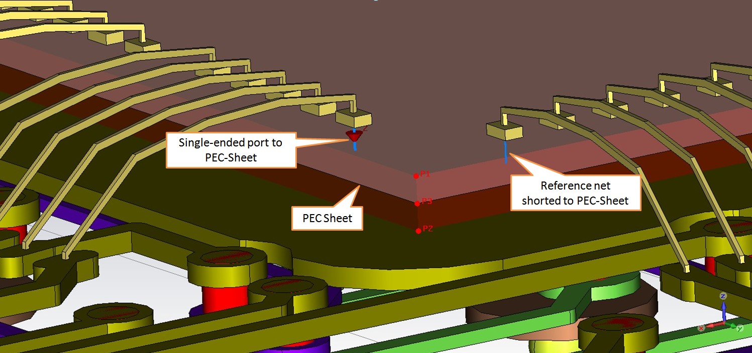
Figure: Automatic port creation using a PEC sheet as a component reference, for a diestack component connected through wirebonds.The selected reference nets are shorted to the PEC sheet.
Lumped-element geometry
A single-ended port can be geometrically represented in one of the following ways.
Edge
The two pins of the lumped element are directly connected by an edge representing the lumped element. If the component elevation is non-zero, vertical pin-leads are used and the lumped-element edge is lifted accordingly.
Face
This is option is similar to the one before, but the construction happens through two-dimensional rather than one-dimension objects.
Edge to component PEC sheet
The lumped element is represented by a vertical edge lumped element and a shorting wire both connecting to the component PEC sheet (see above).
Short-circuit all ground pins on BGA side
This option will introduce a PEC-sheet below (or above) the BGA at a distance specified by the pin-lead height. All component pins that have a net class equal to GND will be shorted to this PEC-sheet.
Specials![]() Mesh
Mesh
Parameters allowing to influence the predefined mesh settings for imported shapes.
Lateral reference length
The imported PCB solids will carry predefined mesh settings. For the computation of the density of mesh lines in x and y directions the present length is used as a reference, see the following option.
Mesh density (x/y direction)
The present option allows to set the size of the minimum x/y mesh step relative to the lateral reference length ("coarse":3, "fine":0.7, "very fine": 0.4). User-specified values different from the predefined ones are also allowed. Please note that global mesh settings may override these settings (e.g. the "Mesh line ratio limit" for hexahedral meshes).
Number of Mesh lines within substrate layers
For hexahedral meshes, the EDA import process will add mesh lines at the top and bottom side of each substrate layer. This enforces the presence of horizontal mesh lines within every conductor layer. In order to improve the mesh resolution within the substrate layers, additional mesh lines can be introduced by choosing values larger than zero in the present option. Again, the global mesh settings may override these settings (e.g. the "Mesh line ratio limit" ).
Consider dielectric die-bricks for simulation
In the default unchecked state, the die-bricks will not be considered for simulation.
Specials![]() General
General
Generate as special PCB Solids
If checked, PCB solids will receive a special treatment in the sense that they are not stored as 3D solids on hard disk. Instead, they are constructed on the fly in the 3D modeler, each time the project history list is executed. As a result, CST project files are smaller and project opening becomes faster. A current limitation is that PCB solids do not appear if the project is included as a subproject. If unchecked, PCB solids are generated once upon import, and are then treated identically to general solids.
Consider dielectric/metal losses
By these switches, the dielectric/metal losses specified in the layer stackup can be turned on or off for the 3D model.
Tool bar
![]() Activate net-selection
mode
Activate net-selection
mode
![]() Activate zoom mode
(the default mode).
Activate zoom mode
(the default mode).
![]() Reset view to whole
board (shortcut: SPACE).
Reset view to whole
board (shortcut: SPACE).
![]() Zoom to selection
(i.e. selected nets).
Zoom to selection
(i.e. selected nets).
![]() Activate pan mode
(if not in pan mode, panning works with the middle mouse button).
Activate pan mode
(if not in pan mode, panning works with the middle mouse button).
 Toggle top/bottom
view.
Toggle top/bottom
view.
 Invert view
colors.
Invert view
colors.
![]() Display pin
names (only relevant if also component outlines are visible).
Display pin
names (only relevant if also component outlines are visible).
 Show grid. The
grid point separation may be set here.
Show grid. The
grid point separation may be set here.
![]() Transparency control
for non-selected objects (applies to etch shapes only). Selected nets
are always displayed with zero transparency. Hiding/unhiding layers changes
the transparency for optimum visibility of selected objects (with the
exception of transparency ="0% (fixed)").
Transparency control
for non-selected objects (applies to etch shapes only). Selected nets
are always displayed with zero transparency. Hiding/unhiding layers changes
the transparency for optimum visibility of selected objects (with the
exception of transparency ="0% (fixed)").
Using the mouse-wheel in the view window
Provides a fast zoom functionality.
The following special characters are used:
* matches zero or more of any character
? matches any single character
[...] matches any single character defined in the character set, e.g. [abcDed] or [0-9]
| (vertical bar) for combining multiple expressions through logical "or", e.g. *gnd*|ground*|vss?
All other characters represent themselves (case insensitive).
See also
Importing and Exporting Models