3D FEFD
Modeling 3D (FE
FD)
3D (FE
FD)
The 3DFEFD solver is based on the frequency-domain Finite-Element method,
combined with a domain-decomposition approach. Special basis functions
are used to take advantage of the planar structures on a PCB. The solver
has been especially designed for the modeling and simulation of typical
power distribution nets existing on high speed PCBs. These type of nets
normally do not consist of thin traces but of wide, stacked conductive
areas. An essential characteristic of the
3DFEFD solver is that it doesn't require a selection
of certain nets. In general, all conductive structures on the PCB will
be taken into account and this significantly simplifies the usage of the
solver.
The dialog box consists of three separate
tabs: two for the Selection of Components and Terminals and one for the
Solver Settings. In the lower left corner the number of the currently
listed components in the Selected
Components list is shown.
Components
/ Terminal Selection tabs:
The present tabs are used for defining the subsets of component-pins
and terminals that will appear at the CST PCB STUDIO
model block. Pins/terminals can be added to the respective lists via drag
and drop from the Navigation
Tree or by using the "Add" button. The usage of the
buttons "Refresh", "Remove", etc. for manipulating
the selection list is described elsewhere (2DTL
Selection tab).
A "selected component" can be further expanded by clicking
on its +-sign, which will display
all corresponding pins. Here, individual pins can be
included/excluded from the modeling (double-click).
Please note that for each selected component, at least two pins must be
included.
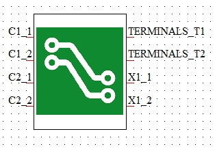
Pressing the
Start
Modeling
button will start the 3D calculation. After the 3DFEFD modeling step
has been performed, the PCB schematic symbol will show all selected component
pins and terminals. The following picture shows the result of selecting
three times two component pins and two terminals.
Solver Settings tab
The present tab is described elsewhere (PI Analysis).