Material Library
Edit Layout Materials
The dialog box is also available via Navigation
Tree: Technology
Materials. A
right mouse click on Materials
opens a drop-down menu where the user is able to call the Edit
dialog box. It shows a list of all available materials.
The icons on the top of the dialog box enable the following actions:
Create a new material
Duplicate a selected material
Import materials from an external Material Library
File
Export materials into an external Material Library
File
Delete unused materials
Delete selected materials

There are two different types of materials: conductor
and dielectric. Each material
requires a unique name that has to be assigned in the field Identifier.
The type of the material can be set in the field Material.
Materials of type conductor are
characterized by their conductivity which has to be set inside the field
Conductivity. The Skin
effect of a conductive material is modeled by using this conductivity
value in combination with the 2D cross-section shape of the corresponding
conductor.
In case of material type dielectric,
there are three further parameters. The field Permittivity
enables the definition of the relative
permittivity and the field Loss
angle tan() enables the definition of the dielectric loss angle.
If the Loss angle differs from
zero a specific Frequency has
to be specified where the given Permittivity
is valid. The loss angle will be assumed as constant
over the whole frequency range (see Model
valid up to frequency).
Ohmic loss modeling
The program approximates the increase
in ohmic resistance and the decrease in internal
inductance over the specified frequency range, from DC up to a
maximum frequency, which is specified via the parameter Model
valid up to frequency (see Model
valid up to frequency). The way that the impedance changes over frequency
depends on the general shape of the conductor. On a PCB the typical shape
type is a flat rectangle. In general, the program distinguishes between
thin rectangle (strips) and circular wire shapes. For both shape types
CST PCB STUDIO provides a solution for the two different kinds of model
interpretation during the circuit simulation (see Circuit
Simulation Aspects)
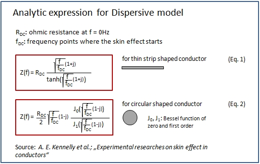
In case of a Dispersive model
interpretation, an analytic expression
is used to describe the Skin effect
over the frequency range:
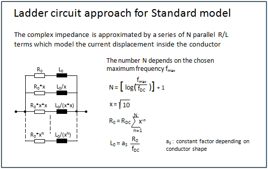
In case of a Standard model
interpretation, a multi-order R/L ladder
circuit approach is used to approximate the characteristic behavior
given by the analytic expression:
Reference:
"Experimental Researches on Skin Effect in
Conductors", A.E. Kennelly; P.H. Pierce, Panama-Pacific Convention
of the American Institute of Electrical Engineers, San Francisco, September
16.th 1915
"Digital Signal Integrity", B. Young,
Prentice Hall, 200, chapters: 7.4 and 10.3
Dielectric loss modeling
The program approximates a constant
loss angle over the specified frequency range, from DC up to a maximum
frequency (see Model
valid up to frequency). The crucial point in dielectric loss modeling
is to keep the model causal.
CST PCB STUDIO provides a solution for the two different kinds of model
interpretations during the circuit simulation (see Circuit
Simulation Aspects)
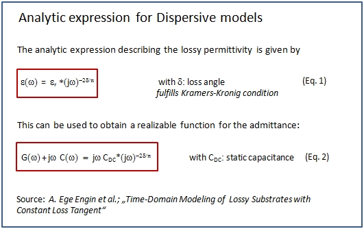
In case of a Dispersive model
interpretation, an analytic expression
is used to describe the relationship between the increase
of conductance and the decrease of capacitance
over the frequency range. At the frequency, specified in the material
definition dialog box, the capacitance corresponds to the permittivity,
also specified in the material definition dialog box.
In case of a Standard model
interpretation, a multi-order Debye approach
is used to approximate the characteristic behavior by the analytic expression:
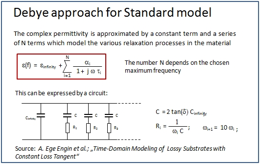
Reference:
"Time-Domain Modeling of Lossy Substrates with
Constant Loss Tangent", A.E. Engin; W. Mathis; W. John; G. Sommer;
H. Reichl, Signal Propagation on Interconnects, Proceedings. 8th IEEE
Workshop; 9-12 May 2004, pp 151-154