
cst 设置的离散端口总是说泡在pec中 无法仿真 怎么弄?
05-08
从图上看 离散端口和pce半毛钱的关系也没有啊!
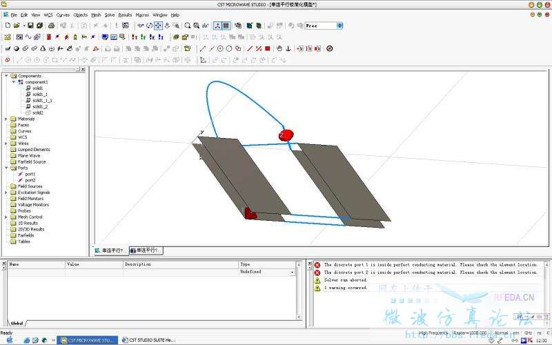
模型就是两传输线并联充电 串联放电,两端口都是s参数激励,我打算提取参数放入pspice电路仿真。
我用一个大的真空长方体把电边界顶开的。
打开背景材料设置(边界条件左边的那个按钮)
将PEC改为NORMAL即可
背景我设成normal了啊 还是一样的 疯了
是不是你的对称面设置的有问题,不是磁或者电对称结构,你设置成对称了
Cannot see the mesh configuration. So please check the following:
You have set up the proper globle mesh configuration or local mesh properties for the PEC. Active the "mesh view" mode and pay attention on the separation area of those PEC pads. Make sure there are sufficient mesh lines between the pads so that the discrete ports won't be merged into PEC in mesh view.
发模型上来就可以了 大家帮忙看看
我也遇到过,我的解决方法是重新设置background material里面的空间扩展,不扩展就ok了,要不就延长,waveguide端口处在边界的边沿。还有就是用deembed port,这个没测试过
源垂直的平面不能电对称
sorry,应该是源所在的平面
检查一下网格设置,可能是网格线设置的太少了吧。
相关文章:
- 请教波导端口馈电尺寸设置的问题.. (05-08)
- CST MWS中端口问题 (05-08)
- 端口设置的问题? (05-08)
- 微带馈电的端口怎么设置 (05-08)
- 端口问题 (05-08)
- 同轴端口的mesh问题 (05-08)
射频专业培训教程推荐