|
微波射频仿真设计 |
|
|
微波射频仿真设计 |
|
| 首页 >> Ansoft Designer >> Ansoft Designer在线帮助文档 |
|
System Simulator > Voltage Controlled Oscillator with Frequency Divider (VCODIVBYN)
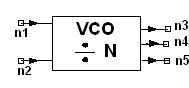
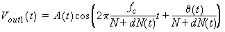
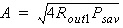
Notes1. This model combines the voltage controlled oscillator with the frequency divider. 2. The pin assignment is as follows: the first input is the tuning voltage signal; the second input (optional, can be left open) is the instant division factor variation dN; the first output is the divided VCO output; the second output (optional, can be left open) is the undivided VCO output; the third output is the phase noise output, it is optional also. 3. The sawtooth waveform type option is valid for baseband output signal only. If the option is set to be sawtooth when the actual signal is a bandpass signal, no action is taken. 4. The parameter “DIV_FLOOR” allows the user to specify noise floor due to the frequency divider. 5. The indexed parameters “FM” and “SBN” allow the user to specify measured noise data. When measured noise data is provided, the model will ignore the parameters QLOAD, F, R, FC. 6. The “FILE” parameter identifies a data file for the phase noise parameters FM and SBN. The filename must have a .dsp extension, and must be in DSP format: xy Where the first column is the frequency offset in Hz and the second column is the sideband noise in dB. For example: xy If a valid “FILE” parameter is present, the data from the file will be used and the corresponding “FM” and “SBN” parameters in the netlist will be ignored. Any “FM” and “SBN” parameters in the netlist that are not also defined in the data file will be used. 7. When the parameter “VcoNoiseOn” is set to 1, VCO noise will be simulated. Otherwise, VCO noise will not be incorporated in the simulation. The same happens to the divider noise. Note that noise simulation is expensive, so when it is not needed, the two parameters should be turned on. 8. Parameters "TSTART", "FRACTION", and "FREF" are used to directly output phase noise data from the third output port. TSTART should be set to a value after the PLL has locked on; this ensures that only steady-state phase noise samples are sent to the phase noise probe. FRACTION is the fractional portion of the steady-state divide- ratio, and should be set to 0 for integer-N PLL designs. Finally, FREF should be set to the reference or comparison frequency that feeds the phase detector. If you choose to use this model without the divider, you must set N equal to 1 and set FREF equal to FLO (Free-running VCO frequency). 9. Assume the output waveform type is set to be
sinusoid. Let the signal from the first input be Vin(t), and the signal from the
second input be dN(t). The relationship between
the inputs and the outputs is given by
A random phase noise process through a filter with a frequency response
9. If the user sets the output waveform option to be sawtooth, then sawtooth signal will be sent to the output with the peak value “A” and the same phase information as the sinusoidal option. 10. If the user supplies the measured V-K data pair, that is the voltage and oscillator voltage gain pair, the tuning sensitivity will be based on the data set instead of the nominal oscillator voltage gain. At the same time, the K value in the noise spectrum calculation will be the average of the supplied measured K values instead of the nominal value. Note that when supplying the V-K pairs, V should be in ascending order. Also, if the actual tuning voltage is smaller than V_1, then K_1 will be used; if the actual tuning voltage is larger than V_n, then K_n will be used. 11. An example using the VCODIVBYN in a fractional-N synthesizer design is provided with Designer. Use the File menu to open InstallDirectory/Examples/System/Motorola_Fractional_Synthesizer.adsn. InstallDirectory is the directory where Designer is installed. See the References under this topic for a paper describing this design and how it was simulated in Designer. 12. To avoid aliasing the VCO output signal, the simulation sample rate should be set to twice the maximum swing of the VCO. This swing is based on the Oscillator Voltage Gain parameter [K] and the maximum allowed tuning voltage of the design.

The VCO output must be a complex envelope signal so you have to also have to make sure your sample rate is less than twice your VCO center frequency [FLO]. In general, your sample rate should be in the range of:

If you are limited by the FLO parameter, you will not be able to simulate the high-end of your tuning voltage range.
Netlist FormVCODIVBYN:Name n1 n2 n3 n4 n5 FLO=val
[FC=val] [QLOAD=val] Netlist ExampleVCODIVBYN:1 1 2 3 4 5 FLO=800MHZ FC=1KHZ QLOAD=200 F=10 + PSAV=0dbm R=5000OH K=1e6 T=290Kel References[1] Wael Al-Qaq, JianHua Gu, William J. Martin, and Jeffrey L. Cutcher, “Fast and Accurate Fractional-N Synthesizer Simulation Using Ansoft Designer™”, Motorola, Inc., Copyright 2004. A PDF version of this paper is provided in: InstallDirectory/Help/Frac_Synthesizer_IEEE_WAMI_2004.pdf where InstallDirectory is the directory where Designer is installed. [2] Ulrich L. Rohde, J. Whitaker, and T.T.N. Bucher, “Communications Receivers” McGraw-Hill, 1996.
HFSS视频教程 ADS视频教程 CST视频教程 Ansoft Designer 中文教程 |
|||||||||||||||||||||||||||||||||||||||||||||||||||||||||||||||||||||||||||||||||||||||||||||||||||||||||||||||||||||||||||||||||||||||||||||||||||||||||||||||||||||||||||||||||
|
Copyright © 2006 - 2013 微波EDA网, All Rights Reserved 业务联系:mweda@163.com |
|

 for envelope
analysis
for envelope
analysis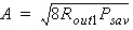 for instantaneous
analysis, and
for instantaneous
analysis, and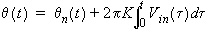 ,
,  is the random phase noise
process, with the power spectral density [1}:
is the random phase noise
process, with the power spectral density [1}:
 is generated by filtering a white Gaussian
random sequence
is generated by filtering a white Gaussian
random sequence  , where
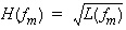
 is a slowly time-varying process.