|
微波射频仿真设计 |
|
|
微波射频仿真设计 |
|
| 首页 >> Ansoft Designer >> Ansoft Designer在线帮助文档 |
|
System Simulator > Voltage Controlled Oscillator (VCO)
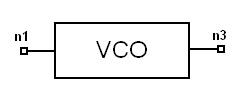
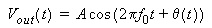
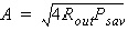
Notes1. This is a Voltage Controlled Oscillator model. It can either output sinusoidal signal or sawtooth signal depending on how the parameter “WAVETYPE” is set. 2. Suppose the output waveform is sinusoid, the relationship between the input and the output is then given by
where analysis, and 3. If the user sets the output waveform option to be sawtooth, then sawtooth signal will be sent to the output with the peak value “A” and the same phase information as the sinusoidal option. 4. The indexed parameters “FM” and “SBN” allow the user to specify measured noise data. When measured noise data is provided, the model will ignore the parameters QLOAD, F, R, FC. 5. The “FILE” parameter identifies a data file for the phase noise parameters FM and SBN. The filename must have a .dsp extension, and must be in DSP format: xy Where the first column is the frequency offset in Hz and the second column is the sideband noise in dB. For example: xy If a valid “FILE” parameter is present, the data from the file will be used and the corresponding “FM” and “SBN” parameters in the netlist will be ignored. Any “FM” and “SBN” parameters in the netlist that are not also defined in the data file will be used. 6. When the parameter “VcoNoiseOn” is set to 1, VCO noise will be simulated. Otherwise, VCO noise will not be incorporated in the simulation. The same happens to the divider noise. Note that noise simulation is expensive, so when it is not needed, the two parameters should be turned on. 7. The power spectral density for this random phase noise process is given by [1]
A random phase noise process If required, linear interpolation is applied in the
time domain on the generated phase noise process 8. To avoid aliasing the VCO output signal, the simulation sample rate should be set to twice the maximum swing of the VCO. This swing is based on the Oscillator Voltage Gain parameter [K] and the maximum allowed tuning voltage of the design.

The VCO output must be a complex envelope signal so you have to also have to make sure your sample rate is less than twice your VCO center frequency [FLO]. In general, your sample rate should be in the range of:

If you are limited by the FLO parameter, you will not be able to simulate the high-end of your tuning voltage range. Netlist FormVCO:Name n1 n2 FLO=val [FC=val] [QLOAD=val] [F=val] + [PSAV=val] [R=val] K=val T=val [FDEV=val] [Seed=val] +[DivNoiseOn=val] [VcoNoiseOn=val] [FM1..n=val] [SBN1..n=val] [FILE='filename'] + [Wavetype=val] [Rin=Val] [Rout=Val] Netlist ExampleVCO:1 1 2 FLO=800MHZ FC=1KHZ QLOAD=200 F=10
PSAV=0dBm References1. Ulrich L. Rohde, J. Whitaker, and T.T.N. Bucher, “Communications Receivers” McGraw-Hill, 1996.
HFSS视频教程 ADS视频教程 CST视频教程 Ansoft Designer 中文教程 |
|||||||||||||||||||||||||||||||||||||||||||||||||||||||||||||||||||||||||||||||||||||||||||||||||||||||||||||||||||||
|
Copyright © 2006 - 2013 微波EDA网, All Rights Reserved 业务联系:mweda@163.com |
|
 for evenlope analysis, or
 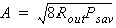 for instantaneous
 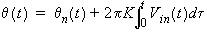 ,
,  is the random phase component at time t.
 is generated by filtering a white Gaussian
random sequence through a filter with a frequency response
is generated by filtering a white Gaussian
random sequence through a filter with a frequency response  , where
 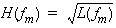 with
with 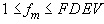
 to ensure it has the same sampling rate
as that of the input signal. In general, the random phase noise process
to ensure it has the same sampling rate
as that of the input signal. In general, the random phase noise process
 is a slowly time-varying
process.
is a slowly time-varying
process.