|
微波射频仿真设计 |
|
|
微波射频仿真设计 |
|
| 首页 >> Ansoft Designer >> Ansoft Designer在线帮助文档 |
|
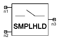
System Simulator > Sample and Hold (SMPLHLD)
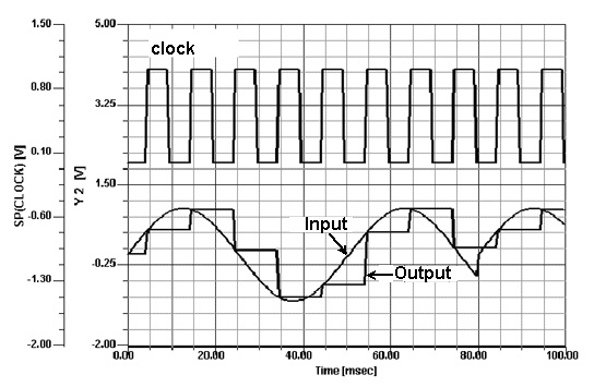
Notes1. The input signal is sampled at each rising edge of the clock signal (the input is sampled at the instant when the clock signal crosses a threshold of 0.5V). In the hold state of the sample and hold the output voltage decays at a constant rate determined by the parameter DECAY_RATE. 2. The output signal is always a baseband signal. 3. The input signal and output signal voltages of the SMPLHLD element, with its CLK pin tied to a clock source with period 10 msec and DECAY_RATE = 0, are shown in the figure below.
Netlist FormSMPLHLD:Name n1 n2 n3 DECAY_RATE=val [Rin1=val] [Rin2=val] [Rout=val] Netlist ExampleSMPLHLD:1 1 2 3 DECAY_RATE=0
HFSS视频教程 ADS视频教程 CST视频教程 Ansoft Designer 中文教程 |
|||||||||||||||||||||||||||||||||||||||||||||||
|
Copyright © 2006 - 2013 微波EDA网, All Rights Reserved 业务联系:mweda@163.com |
|