淘宝官方店     推荐课程     在线工具     联系方式     关于我们  


微波射频仿真设计   Ansoft Designer 中文培训教程   |   HFSS视频培训教程套装


Agilent ADS 视频培训教程   |   CST微波工作室视频教程   |   AWR Microwave Office

          首页 >> Ansoft Designer >> Ansoft Designer在线帮助文档


Ansoft Designer / Ansys Designer 在线帮助文档:


System Simulator >
System Component Models >
Stripline >
   SL Coupled Bend n (SLCBENDSn)       

SL Coupled Bend n (SLCBENDSn)


[spacer]

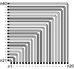
Schematic symbol example SLCBENDSn (n = 20)


Properties

Description

Units

Default

Range

M

Miter ratio

none

Required

[0,1]

W

Conductor width

m

Required

>0

S

Conductor spacing

m

Required

>0

L1

Shift in reference plane 1

m

0

³ 0

L2

Shift in reference plane 2

m

0

³ 0

sub

Substrate name

none

Optional, user defined string

string

CoSimulator

Simulation engine

none

Planar EM

Planar EM

CoSimStackup

Stackup used for simulation

none

Layout Stackup

Layout Stackup, Footprint stackup, Substrate


Notes

1. This model is available for Planar EM simulation only.

2. The default reference plane is typically coincident with the opposing transmission line edge, but is extended if the miter ratio moves the outside edge of the line further out, as shown in the dimensional drawing. The reference plane is shifted even further through the use of parameters L1 and L2.

3. The maximum number of coupled bends is 20.

4. If a substrate is not defined for the component, the Layout stackup or the Footprint stackup may be used.

Netlist Form

There is no netlist form for this component; it is available for Planar EM analysis only.

Netlist Example

N/A


HFSS视频教学培训教程 ADS2011视频培训教程 CST微波工作室教程 Ansoft Designer 教程

                HFSS视频教程                                      ADS视频教程                               CST视频教程                           Ansoft Designer 中文教程


      Copyright © 2006 - 2013   微波EDA网, All Rights Reserved    业务联系:mweda@163.com