|
微波射频仿真设计 |
|
|
微波射频仿真设计 |
|
| 首页 >> Ansoft Designer >> Ansoft Designer在线帮助文档 |
|
System Simulator > Tri-State Phase Frequency Detector (PFDET)
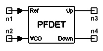
Notes1. This element models the digital behavior of common D flip-flop type tri-state phase-frequency detectors often used in phase-locked loops. 2. The parameters VLin and VHin define the voltage level of the input signal. If an input signal is below VLin, it will be limited to VLin. If the signal is higher than VHin, it will be assumed to be VHin. The output level is set by VLout and VHout in a similar fashion. 3. The threshold at which the phase detector is triggered is determined by (VLin + VHin)/2. 4. This model can handle any type of input signals. The two inputs are usually from a reference oscillator and a divided VCO signal for phase-locked-loop applications. 5. In order to avoid large amount of time jitter and phase noise that would normally be introduced by not using a high enough sampling rate (higher sampling rate means slower simulation), the two output signals can be chosen to be amplitude modulated by setting AMMOD to 1. The so-called amplitude modulation works as follows: if based on the threshold-crossing line, the pulse width should be 1ms but the simulation timestep is 100ms, then the output amplitude or that timestep would be 1% of the VHout value. In detecting the pulse width, linear interpolation is used. Therefore, sawtooth waveforms are recommended. 6. The power spectrum of the noise contribution follows the equation L = Nc+ 10log(Fr) [1], where Fr is the reference frequency in PLL applications and Nc is a constant that is equivalent to the phase frequency detector noise with Fr = 1Hz. 7. When the parameter “NoiseOn” is set to 1, noise will be simulated. Otherwise, noise will not be incorporated. Netlist FormPFDET:Name n1 n2 n3 n4 VLin=val
VHin=val VLout=val VHout=val Netlist ExamplePFDET:1 1 2 3 4 VLin=-1 VHin=1 VLout=0 VHout=1 References1. Ulrich L. Rohde, David P. Newkirk, “RF/Microwave Circuit Design for Wireless Applications.”
HFSS视频教程 ADS视频教程 CST视频教程 Ansoft Designer 中文教程 |
|||||||||||||||||||||||||||||||||||||||||||||||||||||||||||||||||||||||||||||||||||||||||||||||||
|
Copyright © 2006 - 2013 微波EDA网, All Rights Reserved 业务联系:mweda@163.com |
|