|
微波射频仿真设计 |
|
|
微波射频仿真设计 |
|
| 首页 >> Ansoft Designer >> Ansoft Designer在线帮助文档 |
|
System Simulator > Parallel Analog to Digital Converter (PADC)
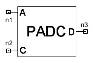
Limits1. VH> VL Notes1. The first input is supposed to be the analog signal to be sampled and quantized, while the second input is the clock signal. On the rising edge of the digital clock input to the parallel ADC, the input waveform is sampled and quantized. The number of quantization levels is equal to 2^nbits, with the range of input values being determined by vl and vh. Input signal values outside of this range will output 0 on the low side and (2^nbits-1) on the high side. 2. If a clock signal is not supplied on n2, the output is clocked out for every incoming sample. Netlist FormPADC:NAME n1 n2 n3 nbits=val vl=val vh=val [Rin1=val] [Rin2=val] [Rout=val] Netlist ExamplePADC:1 1 2 3 nbits = 8 vl = 0 vh = 1
HFSS视频教程 ADS视频教程 CST视频教程 Ansoft Designer 中文教程 |
|||||||||||||||||||||||||||||||||||||||||||||||||||||||||
|
Copyright © 2006 - 2013 微波EDA网, All Rights Reserved 业务联系:mweda@163.com |
|