|
微波射频仿真设计 |
|
|
微波射频仿真设计 |
|
| 首页 >> Ansoft Designer >> Ansoft Designer在线帮助文档 |
|
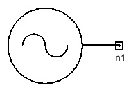
System Simulator > One Port Oscillator (OSC)
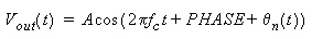
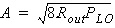
Notes1. All phase noise data must be provided if output is to include phase noise effects 2. In general, the output voltage of this model
is given by:

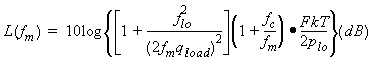
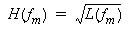
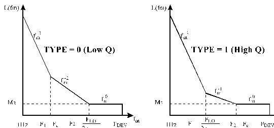
3. The frequency offsets F1 and F2 must be consistent with the specified oscillator TYPE as shown in the phase noise plots below. For a low qload, F1 and F2 correspond to fc and flo/2qload respectively while for a high qload, F1 and F2 correspond to flo/2qload and fc respectively. 4. The indexed parameters “FM” and “SBN” allow the user to specify measured noise data. When measured noise data is provided, the model will ignore the parameters QLOAD, F, R, FC. 5. The “FILE” parameter identifies a data file for the phase noise parameters FM and SBN. The filename must have a .dsp extension, and must be in DSP format: xy Where the first column is the frequency offset in Hz and the second column is the sideband noise in dB. For example: xy If a valid “FILE” parameter is present, the data from the file will be used and the corresponding “FM” and “SBN” parameters in the netlist will be ignored. Any “FM” and “SBN” parameters in the netlist that are not also defined in the data file will be used. 6. When the parameter “VcoNoiseOn” is set to 1, VCO noise will be simulated. Otherwise, VCO noise will not be incorporated in the simulation. The same happens to the divider noise. Note that noise simulation is expensive, so when it is not needed, the two parameters should be turned on. 7. A random phase noise process is generated by filtering a white Gaussian random sequence through a filter with a frequency response H(fm), where
Netlist FormOSC:Name n1 FLO=val PLO=val NSAMP=val SAMPLE_RATE=val + [PHASE=val] [F1=val] [F2=val] [FDEV=val] [M2=val] [TYPE=val] +[DivNoiseOn=val] [VcoNoiseOn=val] [FM1..n=val] [SBN1..n=val] [FILE='filename'] + [SEED=val] [Wavetype=val] [Rout=val]
Netlist ExampleOSC:1 1 FLO=800MHZ PLO=10dbm NSAMP=1000 SAMPLE_RATE=1MHZ + PHASE=90 F1=150Hz F2=10KHz FDEV=100KHz M2=-180dB TYPE=0 References1. Ulrich L. Rohde, J. Whitaker, and T.T.N. Bucher, “Communications Receivers” McGraw-Hill, 1996.
HFSS视频教程 ADS视频教程 CST视频教程 Ansoft Designer 中文教程 |
|||||||||||||||||||||||||||||||||||||||||||||||||||||||||||||||||||||||||||||||||||||||||||||||||||||||||||
|
Copyright © 2006 - 2013 微波EDA网, All Rights Reserved 业务联系:mweda@163.com |
|