|
微波射频仿真设计 |
|
|
微波射频仿真设计 |
|
| 首页 >> Ansoft Designer >> Ansoft Designer在线帮助文档 |
|
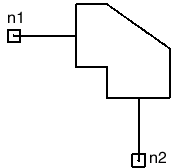
System Simulator > MS Bend, Optimally Mitered (MSBENDO)
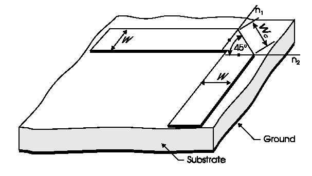
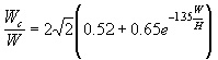
Notes1. Conditions for accurate results are: Frequency £ 18GHz, 2.2 £ er £ 25. 2. The following limitation also applies: W/H ³ 0.25. 3. The miter is 45°
and the length WC is given by: 4. Reference planes coincide with the intersection of the cut with the outer edges of the intersecting lines. 5. Radiation loss is included if cover is not specified. Netlist FormMSBENDO:NAME n1 n2 W=val SUB=label Netlist ExampleMSBENDO:BENDO1 1 2 W=0.025IN SUB=SUB1 where sub1 needs to be defined in the corresponding .sub statement. References1. Wolff, G. Kompa, and R. Mehran, “Calculation method for microstrip discontinuities and T-junctions,” Electron. Lett., Vol. 8, 1972, pp. 177-179. 2. G. Kompa, and R. Mehran, “Planar waveguide model for calculating microstrip components,” Electron. Lett., Vol. 11, 1975, pp. 459-460. 3. T. Okoshi, Planar Circuits for Microwaves and Lightwaves, Springer-Verlag, Berlin, New York, 1983.
HFSS视频教程 ADS视频教程 CST视频教程 Ansoft Designer 中文教程 |
|
Copyright © 2006 - 2013 微波EDA网, All Rights Reserved 业务联系:mweda@163.com |
|