淘宝官方店     推荐课程     在线工具     联系方式     关于我们  


微波射频仿真设计   Ansoft Designer 中文培训教程   |   HFSS视频培训教程套装


Agilent ADS 视频培训教程   |   CST微波工作室视频教程   |   AWR Microwave Office

          首页 >> Ansoft Designer >> Ansoft Designer在线帮助文档
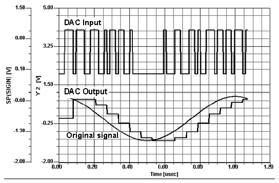

Ansoft Designer / Ansys Designer 在线帮助文档:


System Simulator >
System Component Models >
Data Converters >
   Serial Digital to Analog Converter (DAC)       

Serial Digital to Analog Converter (DAC)


Property

Description

Units

Default

Range/Type

NBITS

Number of bits

None

8

(0, Inf)/Real

VH

Maximum output voltage, in voltage units

Volt

-1V

(-Inf, Inf)/Real

VL

Minimum output voltage, in voltage units

Volt

1V

(-Inf, Inf)/Real

RIN1

Input1 impedance

Ohm

Inf

(0, Inf]/Real

RIN2

Input2 impedance

Ohm

Inf

(0, Inf]/Real

ROUT

Output impedance

Ohm

0

[0, Inf)/Real

Ports

Input1

Input1 bit stream (real)

Input2

Input2 clock input (real)

Output

Output signal (real)


Notes

1. This DAC accepts a serial binary input and converts it into the appropriate analog voltage. At each positive clock edge (when the clock voltage becomes greater than 0.5V) the input signal is sampled and compared to 0.5V to determine if it is a logic 0
or 1. Once nbits bits are clocked into the DAC, the output voltage is calculated. It is assumed that the LSB is clocked in first and the MSB is clocked in last.

2. The figure below shows outputs for an ADC and A DAC with Nbit s= 4, VL = -1V and l = 1V. The clock has a rate of 0.015625 µs, thus, the DAC element outputs a new analog sample every 0.125 µs.

Netlist Form

DAC:Name n1 n2 n3 NBITS=val VL=val VH=val [Rin1=val] [Rin2=val][Rout=val]

Netlist Example

DAC:1 1 2 3 NBITS=4 VL=-1 VH=1


HFSS视频教学培训教程 ADS2011视频培训教程 CST微波工作室教程 Ansoft Designer 教程

                HFSS视频教程                                      ADS视频教程                               CST视频教程                           Ansoft Designer 中文教程


      Copyright © 2006 - 2013   微波EDA网, All Rights Reserved    业务联系:mweda@163.com