|
微波射频仿真设计 |
|
|
微波射频仿真设计 |
|
| 首页 >> Ansoft Designer >> Ansoft Designer在线帮助文档 |
|
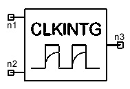
System Simulator > Integrator with Clock (CLKINTG)
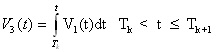
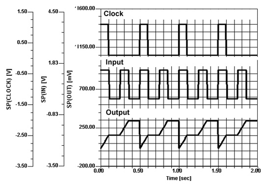
Notes1. This element performs an integration on the
input signal during the time interval determined by the clock signal.
Let T0, T1, T2, … be the time
instances with the positive edges of the input clock, V2(t),
occur (a positive edge occurs at the instant when the clock voltage,
V2(t), crosses a threshold of 0.5V). The output signal V3(t)
is then determined by the following equations in terms of input signal
V1(t).
Netlist FormCLKINTG:Name n1 n2 n3 [Rin1=val] [Rin2=val][Rout=val] Netlist ExampleCLKINTG:1 1 2 3
HFSS视频教程 ADS视频教程 CST视频教程 Ansoft Designer 中文教程 |
|||||||||||||||||||||||||||||||||||||
|
Copyright © 2006 - 2013 微波EDA网, All Rights Reserved 业务联系:mweda@163.com |
|