

Abstract
Understanding the physical behavior of products when several physical mechanisms interact simultaneously becomes increasingly important. By performing coupled simulations including thermal and electrical analysis of devices, engineers are able to predict product behaviors more precisely for changing conditions. CST MICROWAVE STUDIO (CST MWS) allows the user to couple a three-dimensional full-wave analysis with the thermal simulation of the corresponding loss distributions. The following application note gives you a brief introduction into the theory, and it describes the co-simulation of a micro-strip coupler device including the Time-Domain solver and thermal solvers of CST MWS.
Calculate and export thermal losses
In general, coupled simulation (or co-simulation) refers to a combined numerical computation of a system including two (or more) physical effects interacting on the system. For an electrical and thermal co-simulation the electrodynamical and thermal effects determine the resulting behavior of the system. The thermal effects are described by the heat equation, and the electrodynamics of the system is determined by the Maxwell equations. The solver technology included in CST STUDIO SUITE allows you to simulate both effects independently by its corresponding solver modules as well as the coupled interaction from the electrodynamics to the thermal effects. CST MICROWAVE STUDIO therefore allows for a 3D full-wave analysis including losses to simulate the thermal loss distribution, the spatial temperature distribution T as well as the heat flow density.
The transient thermal solver calculates the time dependant heat equation, while the stationary thermal solver does not consider any time dependency:
including sources given by heat sources and thermal loss distributions of the full-wave simulation. In the formulation above P represents sources and losses, K is the thermal conductivity, ρ is the mass density, and c denotes the specific heat. The thermal diffusion equation is solved subject to an initial temperature distribution and boundary conditions.
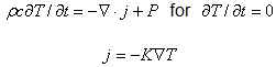
The coupling is set up by deriving two sub-projects from a standard .cst project. Therefore one has to switch to the Schematic canvas which can be accessed by selecting the tab below the main view:
The process of setting up a simulation task in the design environment is described in detail in the document "CST MPHYSICS STUDIO - Workflow and Solver Overview".
After creation the simulation tasks are accessible via the navigation tree:
In principle each simulation task is based on a sub-project with its own geometry, mesh and solver settings. Both simulation tasks are linked by the loss distribution which is computed by the EM task first and then imported by the thermal task.
The general workflow outlined as a checklist is as follows.
Define or import the geometry and define basic material properties in the main project
Derive an EM simulation task from the main project
Define electric material properties in CST MICROWAVE STUDIO
Define electromagnetic
boundary conditions by opening Simulation: Frequency and Boundaries![]() Boundaries and Symmetries
Boundaries and Symmetries
![]()
Define E- and H-field
monitors for volume and surface loss evaluations by opening Simulation:
Monitors![]() Field Monitor
Field Monitor ![]()
Run the electromagnetic field solver (LF-, HF-, Eigenmode-solver,...)
Use the thermal loss
calculation via Post Processing: 2D/3D Field Post Processing![]() Thermal Losses
Thermal Losses ![]() or a postprocessing template to compute and store the thermal loss distribution
or a postprocessing template to compute and store the thermal loss distribution
Derive a thermal simulation task from the main project (this step can also be done together with the creation of the EM simulation task)
Add or modify structure elements if necessary
Define thermal material properties in CST MPHYSICS STUDIO
Define thermal boundary conditions
Specify the loss distribution
for the co-simulation in Simulation:
Sources and Loads![]() Thermal Losses
Thermal Losses ![]()
Consider volume losses and/or surface losses
Set the power scaling factor
Define additional thermal sources (like temperatures or heat sources)
Start the thermal solver
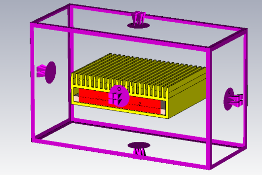
A micro-strip coupler device is examined to demonstrate the electrical and thermal co-simulation. The device consists of a directional strip line coupler inside an aluminum enclosure with a heat sink on the top. The background material is defined as vacuum. Four rectangular waveguide ports are defined at the micro-strip ends for the input and output coupling of the quasi TEM modes. Therefore electric boundary conditions are used for the waveguide ports which is enabled by an electric shielding.
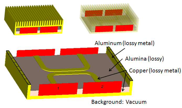
Model of the micro-strip coupler device with four ports.
TEM mode pattern at port 1 of the coupler.
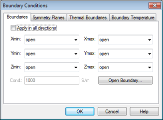
The Time-Domain solver is applied for the simulation of the S-parameters and 3D field monitors using a frequency range of 0 to 1.6 GHz. The operating frequency of the device is 0.9 GHz; the boundary conditions are set to open as shown below.
Boundary condition settings.
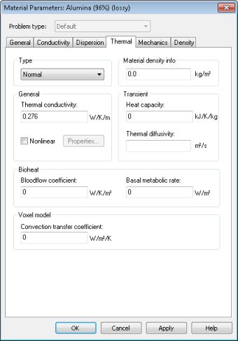
To obtain the electrical volume and surface losses, electric conductivities must be defined for all metal materials, and for normal materials (dielectrics) a loss model must be applied. This can be done by using either constant electric conductivities or by defining electric tangent delta values for the materials.
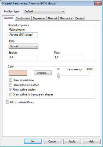
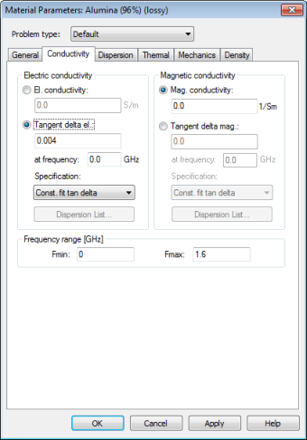
Material parameter settings for alumina
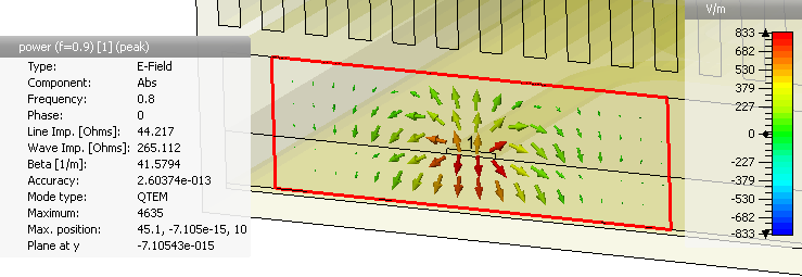
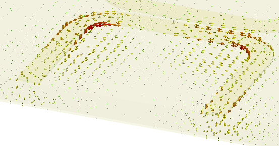
The resulting symmetric field distributions in the coupler device are visualized in Figure 4 and 5 using the 3D E-field and power flow monitors. The directional coupling of the micro-strip device is shown by means of the fields at the operating frequency of 0.9 GHz. Also the current density at 0.9 GHz is shown below.
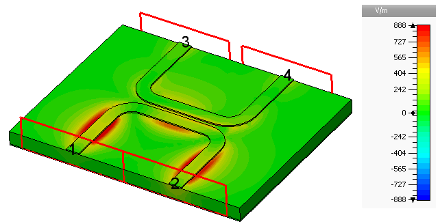
Electric field distribution at 0.9 GHz.
Current density at 0.9 GHz.
The S-parameters are evaluated as shown below. Regarding the high absolute value of the S-parameter S21 the coupling of the field energy from port 1 to port 2 is obvious.
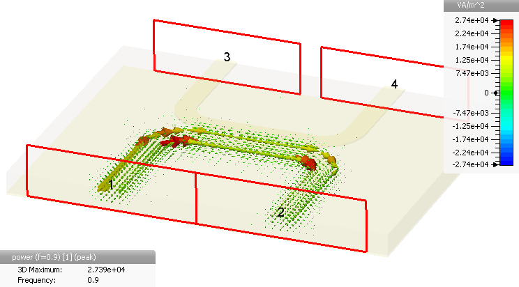
3D power flow through the coupler at 0.9 GHz.
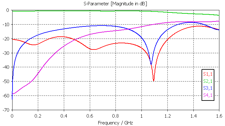
S-parameters
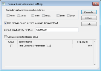
After the EM simulation is finished, the thermal loss distributions needs to be computed and prepared for the Thermal simulation task.
Open the thermal loss calculation settings by selecting
Post Processing: 2D/3D Field Post Processing![]() Thermal Losses
Thermal Losses ![]() :
:
The principle workflow for the thermal simulation is very similar to the EM workflow.
Possible thermal sources for the coupled simulation using CST MPHYSICS STUDIO include
Temperature sources (fixed & floating temperatures)
Heat sources
Biological tissues (bloodflow and metabolic heat sources)
External loss distributions:
Stationary and low-frequency current fields
High-frequency density or loss density fields
Loss distributions from crashed particles (from CST PARTICLE STUDIO).
The definition of the sources can be done in the Sources and Loads section of the Simulation: ribbon:
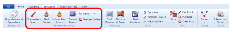
The Sources and Loads section in the simulation ribbon.
In this case the heat sink at the top of the housing is considered by defining thermal surface properties which model a natural convection.
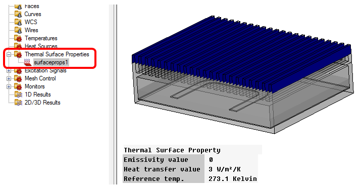
Thermal surface properties for a natural convection boundary condition at the heat sink comb.
The device is driven with 25 Watt input power causing the thermal losses - therefore the loss distribution from the EM simulation task needs to be imported (via Solve -> Thermal Loss Distribution...).
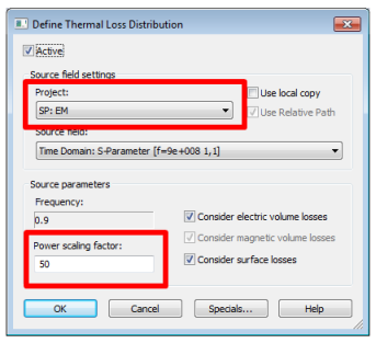
Note: In order to obtain an input power of 25 Watt, the power scaling factor (RMS power) is set to 50 since the transient solver uses 1 Watt peak power for excitation.
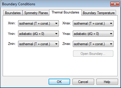
The boundary conditions for the thermal simulation can be either isothermal (T = const.) or adiabatic (dQ = 0). In addition, open boundary conditions can be applied. The heat flow Q of the temperature behaves as follow: for isothermal boundaries the tangential component of Q vanishes, for adiabatic boundaries the normal of Q is equal to zero at the boundary.
All materials of the simulation model in the Thermal simulation task must be defined having thermal conductivity properties if losses occur in these regions.
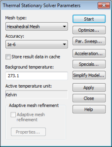
After the thermal setup was completed the stationary solver can be started
Various simulation results of the thermal simulation task can be accessed via the Result Tree as shown below:
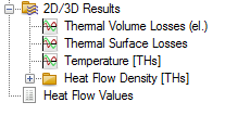
Result tree after the thermal simulation task was finished
The thermal volume losses imported from the EM simulation task are shown below. The losses can be visualized by using the option 3D Fields on 2D plane.
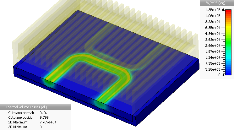
Thermal volume losses (logarithmic plot)
As a result of the coupled simulation, a higher temperature as well as a bigger loss density is given in the direction from port 1 to port 2 in the alumina substrate.
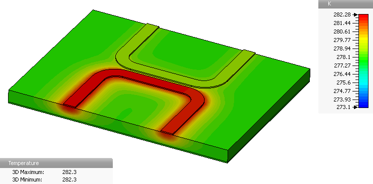
Temperature distribution of the micro-strip coupler device.
Note that the material with the highest losses but smallest thermal conductivity shows the biggest increase in the temperature. Below the temperature for a vertical cross section is shown so that the temperature decay due to the heat sink at the top of the device is evident.
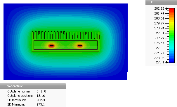
Temperature distribution shown in a vertical cross section. The temperature decay due to the heat sink at the top of the device is visible.
In addition to the results shown above, the heat flow for the surface and volume losses, respectively, and the heat flow density are given as simulation results in a text file.

The study demonstrates how to couple an electrical- and a thermal analysis for a micro-strip coupler device within the CST STUDIO SUITE. The coupler shows a characteristic directional coupling behavior in the electrical analysis. The following thermal simulation exhibits the corresponding thermal loss and temperature distributions.