

This type of block implements a T-junction in a microstrip. The following figure illustrates the layout.
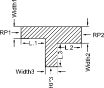
The reference planes are marked RP1…RP3 in the above diagram.
The block is characterized by the properties listed below. To modify the values, use the Block Properties – Parameters dialog box. The common substrate properties are defined by a Microstrip Reference Block.
|
Width1 |
Width of the trace at port No. 1 |
|
Width2 |
Width of the trace at port No. 2 |
|
Width3 |
Width of the trace at port No. 3 |
|
Length1 |
Length of the transmission line at port No. 1 |
|
Length2 |
Length of the transmission line at port No. 2 |
|
Length3 |
Length of the transmission line at port No. 3 |
|
Layer |
Index of the reference block layer that is used by the metallization of this block |
The properties listed above and the substrate properties of the reference block define the electrical behaviour of the block. The layout view uses another set of layout properties. These properties define the position of the block in the layout view. The electrical behaviour of the block does not depend on these properties.
The implemented equivalent circuit model was developed by Hammerstad.
See also
Block Overview, Microstrip Reference Block, Layout Properties