

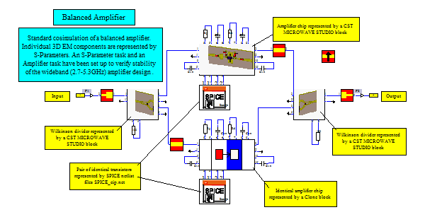
For a balanced amplifier design two simulation tasks have been set up. An S-Parameter task and an Amplifier task to verify the stability of the wideband (2.7-5.3GHz) design.
The model comprises several 3D EM components, namely, a pair of amplifier chips and two different Wilkinson dividers at the input and output for power combining. Because the two amplifier chips are identical, a clone block is used to clone the behaviour of the CST MICROWAVE STUDIO parameteric block, representing the amplifier chip. The two amplifying devices are represented by SPICE netlists that have been extracted, using the Network Parameter Extraction tool in CST DESIGN STUDIO. Certain parts of the geometry have been absorbed into microstrip blocks. The so-called standard cosimulation approach is applied where all individual components of the design are characterised by scatteing parameters in the frequency range of interest. The input port is port 1 and the output port is port 2.