
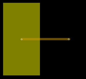
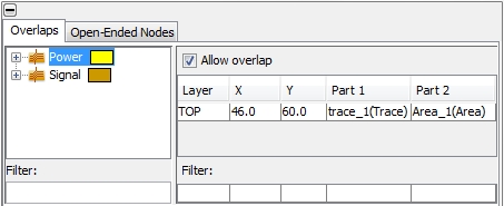
Layer: Displays the layer where the overlap occurs
X, Y: The coordinates where the overlap occurs. This point is just the average of all points where the overlap occurs. The whole overlapping area is not shown.
Part 1: The substructure (trace or area) of the first net (intersecting the second net)
Part 2: The substructure (trace or area) of the second net (intersecting the first net)
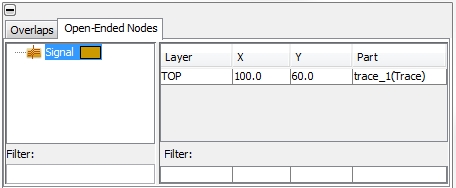
Layer: Displays the layer where the open end occurs
X, Y: The coordinates where the open end is located
Part: The substructure (trace) where the ope end is located.