Layers Stackup
Check Layout Stackup
All PCBs have got a certain layer stack with a particular number of
layers. Although the number of layers is normally defined in the PCB design
input files, the corresponding layer stack itself (the so called
technology) is often not. If the technology
is defined in the PCB design input file(s) it will
be automatically imported during the EDA import. If the technology is not defined,
then certain default values will be used during the import and since the
stack up technology has a big influence on the high frequency behavior,
it should be reviewed after a PCB import in any case. The
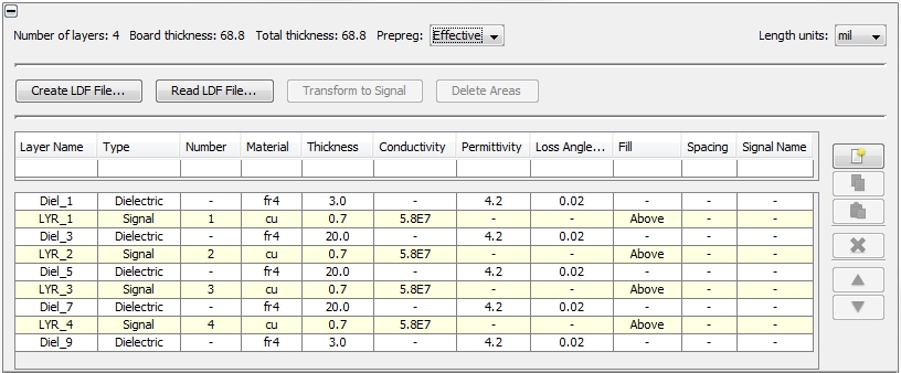
Stackup Manager shows all layers at a glance:
Some of the parameters in the tabular view can be edited. This is possible
by double-clicking on the corresponding item and after that by entering
the new value or changing the selection in the appearing pull-down menu.
Certain parameters like Number
(third column) can’t be changed because they are set automatically.
Number of layers: Displays
the number of all conductive layers in the stack up.
Board thickness: Displays
the overall thickness of the PCB. The value depends on how the thickness
of the dielectric layers is interpreted. There are two different options
which can be selected in the field Prepreg.
Length units: Defines the unit
for all geometric length values.
Total thickness: The total
thickness is the sum of the Board thickness
and additional, artificial layers. There are two kind of artificial layers:
Enclosure and Mirror
Plane which are explained at the bottom of this page (see Create
New Layer).
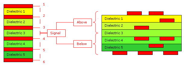
Prepreg: Defines how the thicknesses
of the dielectric layers are interpreted. There are two possibilities:
Effective or Nominal and the difference is explained in the figure
below:
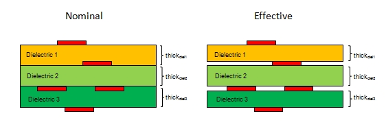
In case of Nominal
the thickness of the dielectric layers are interpreted from the lower
dielectric interface to the upper dielectric interface. The conductive
structures of a signal laying along a dielectric interface are impressed
in either the dielectric layer above
or below. This can be chosen within
the column Fill. The overall board
thickness is the sum of all dielectric layers plus the two signal layers
at the top and bottom of the board. No inner signal layer contributes
to the board thickness. A disadvantage of the Nominal
interpretation is that the distances between two conductive layers are
not given directly.
In the case of
Effective the thickness
of a dielectric layer specifies the distance between the attached conductive
layers. The filling of the void space inside the conductive layers is
not fixed by the given data. The filling actually happens through flow
processes from the adjacent dielectric substrates during the manufacturing
process. Naturally the nature of the dielectric layer (Core
/ Prepreg) determines how the
void filling happens. Here, the program automatically fills the void space
according to the above / below specification inside the column Fill.
The overall board thickness is the sum of all dielectric and all signal
layer. The advantage of the Effective
interpretation is that the distances between two conductive layers are
given directly by the thickness of the corresponding dielectric layer
in between.
Most of the EDA design tools provide the dielectric layer thickness
data according to the
Effective specification.
But it is recommended to assure the setting for every new PCB project,
because the interpretation influences the high-frequency behavior of the
layout.
Create LDF File...: Offers
the export of the current layer stack up definition into a Layer
Definition File.
Read LDF File...: Offers the
import of an existing Layer Definition
File. When reading a LDF
file, the number of layers are automatically checked the user is prompted
if the number of layers mismatch.
Layer Name: Includes the name
of the layers which are also displayed in View Options Window. The fields inside this
column can be edited.
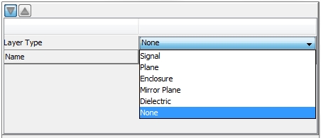
Type: There are three types
of layers: a dielectric type called
Dielectric, and two conductive
types: Signal and Plane.
The fields inside this column actually can not be edited. But in case
of a conductive layer, there is the possibility to switch between the
default setting Signal and the
optional setting Plane.
Transform to Signal
and Delete Areas
Sometimes it is useful that all non-conducting areas on a conductive
layer with different signal structures (traces, areas and vias) can be
filled with metal. This can be done in a three-step procedure which is
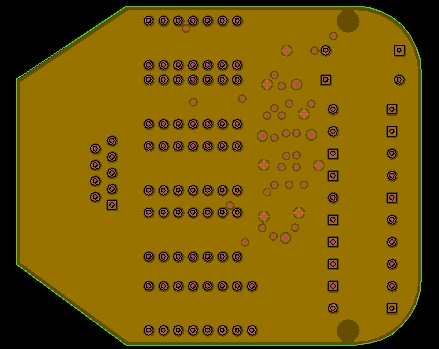
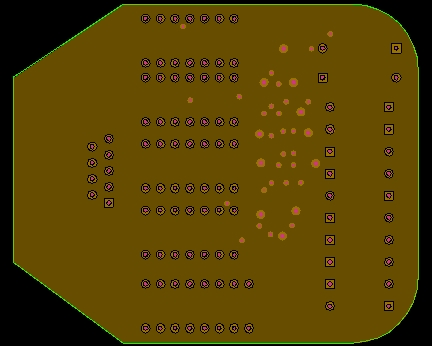
explained in the following example. The figure below shows a metallic
layer with two bigger drill holes at the top and the bottom side. The
layer should be repaired by removing the two drill holes.

Step 1:
The corresponding layer type in the
Stackup Manager has to be switched to Plane
as shown in the figure below:
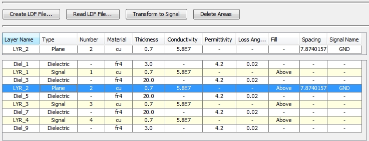
After doing so, two additional buttons called Transform
to Signal and Delete Areas are automatically activated. Furthermore,
the last two columns Spacing and
Signal Name are activated. There
is a default Spacing value of
7.87 mil (= 0.2 mm) and the new
metallic structure has been given the default name GND.
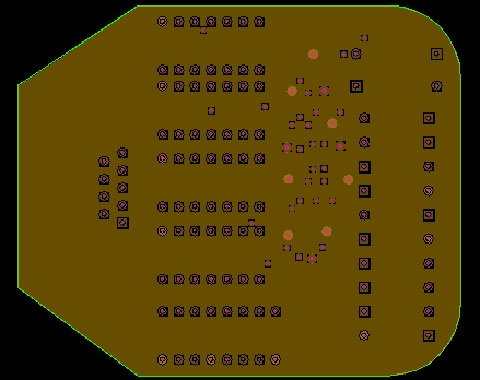
The Main View
shows the new filled metallic layer in overlap with the old structures:
Step 2:
Now, all areas from the old layer definition shall be removed. This can
be done by pressing the Delete Areas
button. After doing so the program informs the user on the number of deleted
areas and after pressing OK,
the new layer can be seen in the Main
View:
.
The drill holes has been removed but now, all signal
vias (and in case of existing traces, traces too) are electrically connected
to the new metallic structure with the signal name GND.
Step 3:
In order to isolate the still existing traces and vias which belong to
other nets than GND, the Transform to Signal button has to be
pressed. After doing so, the non-GND
vias are isolated by the given spacing distance again as shown in the
figure below:
Number: Displays the number
of the metallic layer. The fields inside this column can not be edited.
Material: Displays the material
of the corresponding layer. The fields inside this column can be edited.
Thickness: Displays the thickness
of the layers. In case of a dielectric layers, this value is interpreted
differently according to the settings in the field Prepreg.
The fields inside this column can be edited.
The minimum thickness of any inner
dielectric must be bigger than the sum of the adjacent signal layers.
If this condition is violated an error message will be prompted.
Conductivity: Displays the
conductivity for the metallic layers. The fields inside this column can
be edited.
Permittivity: Displays the
relative permittivity of the dielectric layers. The fields inside this
column can be edited.
Loss Angle tan(): Displays
the loss angle of the dielectric layers. The fields
inside this column can be edited.
Fill: Determines if a trace
or an area on a signal layer shall be embedded into the dielectric above or below the corresponding dielectric interface.
This has a direct influence on the mutual distance between the single
signal layers as the following image illustrates.
The left side of the picture shows a layer stack where
each signal layer is separated from the other signal layers by exactly
one dielectric layer in-between. At the right side of the picture the
resulting geometry is shown if the top three signal layers are of fill
type Above and the bottom three signal layers are of fill
type Below. In order to give an example: signal layer 1
is placed on top of dielectric layer 1 and embedded into the environment dielectric
(e.g. air). Signal layer 4 is placed on the bottom of dielectric layer
3 and embedded into dielectric layer 4.
Note: The interpretation
of the thickness of the dielectric layers is determined by the settings
inside the field Prepreg.
At the right hand side of the Layer Stackup table there is a list of
buttons enabling a convenient handling of the layers inside the table:
Create New Layer: Will be explained
below
Copy Selected Layer: Allows the user
to copy an existing layer
Paste Selected Layer: Allows the user
to paste the previous copied layer
Delete Selected Layer: Deletes the selected
layer
Move Layer Up: Moves the selected layer
upwards
Move Layer Down: Moves the selected
layer downwards
Create New Layer: Pressing this icon
will open the following dialog box:
The dialog box allows the creation of different types of layers:
Signal
Plane
Enclosure
Mirror
Plane
Dielectric
Enclosure:
An enclosure layer is similar to a signal layer: any number of enclosure
layers can be added to the layer stackup, separated by dielectric layers,
of course. The difference to signal layers is, however, that enclosure
layers lie outside the board geometry, above the top layer or below the
bottom layer of the board. An enclosure layers may include any arbitrary
conductor geometry including areas, traces or vias. In this way one is
able to replicate metallic enclosures that cover printed circuit boards.
Mirror Plane:
A mirror plane is a perfectly grounded infinitely expanded metallic layer.
Mirror planes are not subdivided into finite elements for modeling and
simulation but treated in an analytical way (Green’s functions)
by using mirror charges or mirror currents. That is the most effective
procedure to deal with large ground reference planes. Of course, all capacitances
and inductances between the PCB, any enclosure and the mirror planes are
automatically considered. A maximum number of two mirror planes can be
defined only.