Plane Wave
 Sources and Loads
  Plane Wave Plane Wave
Within this dialog, you may define a plane wave excitation source.
Unlike discrete ports or waveguide ports, no S-parameters will be calculated.
Instead, the stimulation amplitude (unit is V/m) is recorded. To obtain
further information, you might specify probes
or different types of field monitors.
Combined with farfield monitors, the plane wave source can be used to
compute the radar cross section (RCS).
Polarization frame
Here, you may enter
the polarization of the plane wave and polarization specific settings.
For more information on the different polarization types, please see the
Plane
Wave Overview.
Linear / Circular
/ Elliptical: Select here the type of plane wave excitation polarization.
Ref. frequency:
If the selected type is circular
or elliptical, enter here the
reference frequency for the plane wave excitation. This field only applies
to elliptical and circular
polarized plane wave excitations.
Phase Difference:
Enter here the phase difference between the two excitation vectors for
elliptical polarized plane waves. This field only applies to elliptical
polarized plane wave excitations.
Left / Right:
Select here between left circular polarized or right circular polarized
plane wave excitation. These settings only apply to circular
polarized plane wave excitations. The respective radio buttons are only
visible if a circular polarization is selected.
Axial ratio:
Defines the ratio between the amplitudes of the
two electric field vectors used for elliptical polarization. This field
only applies to elliptical polarized
plane wave excitations.
Propagation normal frame
X/Y/Z:
Here you can specify the propagation vector by entering valid
for the X/Y/Z component.
Electric field vector frame
X/Y/Z:
Specify the electric field vector components in V/m. The electric field
vector must be orthogonal to the propagation normal. If this is not the
case, the user is asked if the electric field vector components should
be automatically orthogonalized.
Please note that the input signal of an excited
plane wave is normalized
due to the defined absolute value of the electric field vector.
For a circular polarization, the length of the
electric field vector defines the amplitude of the signal. For an elliptical
polarization, the length and the direction of the electric field vector
define the length and direction of the major axis. The length of the minor
axis is computed from the axial ratio given by the user.
|
|

|
|
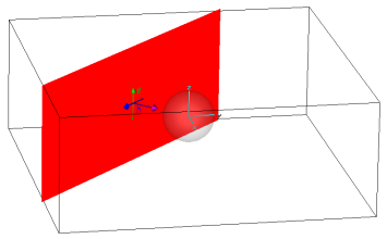
The definition of the plane wave is visualized by a red plane. Colored
arrows indicate the propagation direction as well as the electric and
magnetic field vectors. |
Here the electric field vector of a plane wave is hitting a metallic
sphere. Correspondent to the picture on the left side the plane wave is
excited with an electric field vector in z-direction and a propagation
normal (1,1,0). |
Decoupling plane frame
If a structure contains metallic walls dividing
the calculation domain into two separate parts, it is necessary to consider
a decoupling plane in the plane wave calculation. Note that this decoupling
plane needs to be aligned with the Cartesian coordinate axes (see also:
Plane
Wave Overview ).
Automatic detection:
The selection of this checkbox will automatically detect possible metallic
walls and consequently activate the corresponding decoupling plane. This
detection procedure only recognizes a metallic plane with no discontinuities
at the boundary of the calculation domain. If the decoupling plane is
not found, you may specify a decoupling plane using the input fields below.
Use decoupling
plane: This checkbox is only available if the automatic detection
is deselected. Activate here a user-defined decoupling plane defined by
the following input fields.
Position:
Set the position of the decoupling plane with respect to the plane
normal by entering a valid .
If the metal plane has a finite thickness, specify the surface of reflection.
Plane normal:
Select a normal direction for the decoupling plane. Decoupling planes
need to be aligned with the coordinate axes, so you can choose among X, Y
or Z.
OK
Accepts your settings and leaves the dialog
box.
Cancel
Closes this dialog box without performing any
further action.
Help
Shows this help text.
See also
Transient
Solver Overview, Farfield
Overview, Monitors, Probe
Plane
Wave Overview, Reference
Value and Normalization


HFSS视频教程
ADS视频教程
CST视频教程
Ansoft Designer 中文教程
|
