 Model Parameters
This window is used to set some general model parameters.
The Data id is a title for the model that will be displayed in result plots.
The Units can be chosen between micron, mm, cm, m, mils, inches, or feet. The user should choose sensible units for the model to keep the minimum feature size above 1e-5 and the overall size below 1e5.
The frequency range of interest should be specified here. The Maximum frequency is used by Build to give a default mesh capable of accurately modelling the electromagnetic fields at that frequency.
The Duration for which the electromagnetic environment is analysed can be specified either in seconds or as the distance that a wave will travel in free space during the time of the analysis. If a Residual energy value is defined, then the analysis will be terminated earlier if the specified system energy level is reached before the Duration.
The Maximum frequency and Duration will be defaulted to values according to the size of the model. If the Units are changed prior to editing the Maximum frequency and Duration, then the default values will be changed accordingly.
The Materials window is used to attach materials to geometric bodies. All bodies with materials attached will then be mapped into the analysis file when the model is discretized.
A number of different material types are available on different tabbed pages of the materials window.
Some material definitions can only be attached to particular geometry types. Metal and absorbing panel material can be attached to both solid and thin bodies; dielectric and debye materials can be attached to solid bodies only; and thin panel material can be attached to thin bodies only. The Query tool can be used to check whether a body is suitable for a particular material type. Alternatively, press Q on the keyboard and hover the mouse over an object to see its summary.
Towards the bottom of the Materials window is a list of solid or thin bodies in the model and the type and name of any materials which are attached to the bodies. To the right of this are Attach and Detach buttons that are used to attach or detach defined materials to/from the bodies. Multiple entities can be selected on which to perform the Attach and Detach operations.
A body that has no material definition is ignored and will not be written to the TLM file.
At the bottom of the dialog are two buttons to Load material file and Save material file. The user may have a number of materials that are used in several different models. Rather than having to define the materials each time a new model is created, the user can compile a library of materials, save them to file and load them into the pages of this window. The Save material file button writes all materials to file, regardless of whether they are attached to any bodies and so can be used to incrementally add to the material file.
Each time a model is opened, Build reads the materials.sat file typically stored at C:\Program Files (x86)\CST STUDIO SUITE 2010\Library\MS for the list of materials tio show.
Each tabbed page contains a list of materials available and buttons that are used to Create, Modify and Delete materials in the list. Modifying a material definition alters the material definitions already associated with bodies. The user may Delete a material definition that has been assigned to a body in the model and this will result in the material definition being detached.
Metals can be defined either by Surface impedance or by Conductivity and Relative permeability. Surface impedance gives a frequency independent loss. The definition of conductivity leads to a frequency dependent skin depth model. The additional computational effort to represent materials with loss is negligible.
Metals may overlap dielectrics in which case the region of overlap is taken to be metal. This feature is useful when metal parts are embedded in dielectric medium.
Dielectrics can be isotropic or anisotropic. On selecting the Anisotropic check box, two extra columns appear for each property. The three columns are used to enter the properties pertinent to the x, y and z directions for each of the Relative Permittivity, Relative Permeability and Conductivity. Instead of defining the Conductivity, the user may choose to define the Loss tangent at a particular frequency. The program will then calculate the appropriate conductivity value and store it in the material definition.
Debye materials are Frequency Dependent Materials that can be applied to solid volumes. Load the material definition file tissues.sat for an example of how these materials are defined. Tissues.sat contains the Debye representation of some human tissue types.
Thin Panel Materials have the same Relative Permittivity, Relative Permeability and Conductivity as dielectrics (though they are only isotropic), as well as a Thickness. The thin panel material should only be attached to a sheet body not to a solid body.
Thin panels may have a number of poles that are used to define how the permittivity and permeability change with frequency. When the user selects a material in the list at the top of the page, the poles are displayed for that material, and can be edited or added to.
Absorbing Panels material is used to represent absorbing tiles. The material properties are the same as for Debye material, but the absorber thickness must also be defined. The Absorbing panel is a layer of absobing material that is metal backed - no signal will penetration beyond it.
Cable material is a definition of Shielded cables that can be attached to any wire. The wires with the material attached are then converted to shielded cables, containing a single inner conductor. Wires without a cable material attached are treated as bare.
The shielding properties of the cable are defined using a Transfer impedance model. The Resistance and Inductance per unit length of the shield are required.
If shielded cables are included in a model, the terminations of the inner conductor of the cables are matched during the 3D simulation, and the solver will obtain the current at these matched terminations. A post-processing tool, called Shielded Cable Solver, is used to apply simple non matched terminations to the inner conductor after the 3D simulation.
Using matched terminations during the 3D simulation prevents the inner conductor from resonating, and minimizes required run time for the 3D simulation. If you wish to change the termination impedance for the inner conductor of shielded cables, select Settings in the Navigation tree.
It should be noted that the diameter of the shielded cable inner and outer conductor are always in metres.
The Mesh Definition window consists of multiple pages. The first page is for setting the automatic mesh rules, the second is for refining the mesh over bodies and defining the lumping rules, the last three pages list the definition of the mesh in the X, Y and Z directions.
The extents of the mesh can be defined with a percent space around the model, or by fixing the extent with a location. Fixing the position of the mesh extent is typically only done for specifying symmetry conditions.
By default all extent values are set to 0%, which means the mesh is tight around all geometric entities in the model. The extension percentage is based on the largest axial dimension of the device. For example, a 50% extension around a device that is 10x10x100 would give a mesh that is 110x110x 200 (an extension of 50 units in each direction).
The extents can also be defined as a percent of a wavelength at a frequency of interest. This is particularly useful for electrically small devices.
The boundary conditions on the six faces of the mesh are defined in this window. The possible choices are Absorbing, Electric wall, Magnetic wall and Wrap around.
Electric wall is used to enforce no transverse electric field (like a perfect metal sheet).
Magnetic wall is used to enforce no transverse magnetic field.
Wrap around connects two opposite boundaries with a no phase shift. So that any signal that propagates out of one boundary reappears at the oppositve boundary. This condition only has any meaning when applied to both sides of the mesh, so if the Minimum x condition is set to Wrap around, the Maximum x will automatically get set to that.
Under the Advanced button the user has the choice of using perfectly matched layers (PML) or not for the Absorbing boundaries. If PMLs are used then a number of layers defining the PML depth must be specified in terms of numbers of cells and care should be taken to ensure that the PMLs do not overlap other entities in the model. It is recommended that you set the number of PML layers as 8. Keep in mind that these PML layers will be filled in from the outer boundary of the existing mesh, so care should be taken to ensure that the PML does not overlap the model geometry or output regions. It is recommended that you do not use PML boundaries.
Also on this advanced window is the Boundary proximity rule check box that is used to specify whether the electromagnetic simulator accepts bodies within 30% of the mesh extents when absorbing boundaries are applied.
By default the 3D-TLM Simulator will not check for overlapping material with different properties. This check can be enabled by unticking Allow different materials to overlap.
A Ground plane beyond the mesh can be defined on the Advanced window. This enables the effect of a distant ground plane to be included in results generated in the near and far field, and monitor points outside the mesh. This means that the reflection from a ground below the model can be included, without the need to extend the mesh down to the ground plane.
In the Options section of the Mesh definition window, the user can choose what features the mesh should be aligned (or snapped) to, and what mesh refinement is required. Check boxes can be ticked or unticked to snap cell faces onto planar faces, straight edges, or points of body in the model that have material characteristics.
The number of cells required across axially aligned faces in the model can be set. If the Refine Faces check box is on, then subject to the minimum cell size constraint, the mesher will place the specified number of cells across each axially aligned face, with a small number of equally fine cells on either side of the face.
If the Refine cylinders check box is on, then any axially aligned, closed cylinders will be refined. The mesher ensures that the cross-sectional maximum cell size within the bounds of the cylinder is no greater than the diameter divided by the Number of cells across diameter value. This is imposed in the transverse directions of the cylinder, not in the axis direction.
The user can also impose a similar refinement of arcs (closed circular edges) for cases such as a circular hole in a planar sheet body.
The wavelength at the maximum frequency is shorter within dielectric than in air. Dielectrics are always refined to ensure that the maximum cell size within all dielectric bodies is sufficiently small to obey the 10 cells per wavelength rule.
If the Refine edges check box is on, the mesher will inspect the model for any edges, and place finer cells in the vicinity of those edges. The cell size chosen is by default either no larger than the actual smallest cell size used elsewhere in the mesh, or if Wanted minimum cell size is selected, the mesher will refine edges according to the defined minimum cell size for the model
Tick Smooth mesh to get more gradual variation of cell size across the mesh. This generally improves accuracy.
At the bottom of the window are the controls for the Maximum and Minimum wanted cell size near to the model. The maximum wanted cell size is defaulted at the value needed to accurately model the electromagnetic fields at the maximum frequency specified in the Model parameters window. The rule used is the smallest of 10 cells per wavelength or 5% of the device size. The latter limitation is intended to provide a better mesh for electrically small devices. This cell size will be used over the model. For space between the model and boundaries of the mesh, the Cell size wanted far from model on the Refine tab of the Mesh dialog will be used.
The Number of cells in the mesh and Number of timesteps are displayed at the bottom of the window, these have a direct effect on the solver run time. The number of timesteps required is inversely proportional to the minimum cell size so effort should be made to prevent the minimum size being too small.
To ensure the mesh is automatically calculated whenever the geometry is changed, leave ticked the option to Automesh, below the Settings page.
The Refine tab is used to define a maximum cell width and minimum buffer size for any bodies in the model, and the lumping controls. These value will then be used by the Automesher.
Click Add to add bodies in the model to the refine list, or in the model view or Navigation tree, right click and select Refine.
The maximum cell width and buffer can be applied in the x, y and z directions.
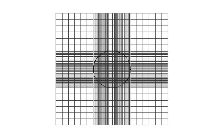
The nature of aCartesian mesh definition is such that refinements cannot be applied locally but will affect cell size across the width of the mesh, as illustrated in the example of a cylinder below. Outside the cylinder, fine cells are not needed. The coarser cells that are seen in the corners of the picture would be sufficient.
For further information on lumped cells, please refer to Lumped Cells.
The Lumped cells mechanism groups adjacent cells into one larger cell, reducing the amount of work for the solver, see Lumped Cells.
It is recommended that cell lumping is always set to automatic, in which case, cells are automatically lumped together at locations distant to fine geometric features.
Consider carefully the value of the maximum cell size far from model for waveguide devices. This cell size will be used for the lumping and due to the rapid field variation often seen within waveguides, quite often you will want to use a cell size smaller than 10 cells per wavelength here.
X, Y, Z pages
The X, Y, Z pages list the cell sizes in the three axis directions. These values can be edited if Automesh is unticked, but this is not recommended.
The mesh is defined, in each direction, by one or more cell sets. Each set represents an interval on one of the axes, and the fineness of the mesh is controlled by the number of cells specified within that interval.
Along a given axis, all cells within a set have the same dimension in the axial direction. The cell sets must be continuous, so that the maximum position of one cell set is equal to the minimum position of the next along that axis.
At the top of each X, Y, Z page is a list containing cell sets that have been defined. This shows the range of the cell set (Minimum and Maximum), the number of cells in the set (No. of cells) and the width of each cell (Cell width). New cell sets are created by adding cell set boundaries at the Cell face on x = value using the Insert button. Cell-set boundaries are removed at that value using the Delete button. The range and number of cells of a set can be altered by selecting that set in the list, editing the boxes in the Edit set area and pressing Apply.
The Ports window consists of a list of ports that have been defined in the model. The user can Create new ports, Modify existing ports, or Delete them.
Various port types are available, listed below.
The Excite all simultaneously check box indicates whether all ports are excited in one job, for example to excite all elements of an antenna array, or all ports are excited in separate jobs to obtain scatter parameters.
For 2 port devices that have symmetry, you turn off the excitation for one of port using the Details button, and define the symmetry condition used in post processing in Settings on the Navigation tree.
If Excite all is ticked you can change the amplitude and time or phase delay to steer an antenna array.
Move ports is used to shift the reference plane at which the port scatter parameters are calculated. Note the actual normal position of the reference plane should be defined, not the distance moved.
Rectangular TE ports can be defined within a rectangular, axially directed waveguide. The cross-section is defined by the Ingoing Direction, Minimum and Maximum points. These can be entered manually or the Pick inner loop button can be used to obtain the parameters from the model view by picking any edge in the end profile of the waveguide.
Next, the user should choose the mode that is associated with the port. The Cutoff frequency is calculated and indicated on changing the selected mode. If the user has picked an inner loop, then that action will automatically select the mode with the lowest cutoff frequency. A useful trick for double ridge waveguides is to set this cutoff frequency to -1, which is an instruction to the solver to automatically determine the fundamental mode cutoff.
Circular TE/TM ports can be defined within a circular, axially directed waveguide. The cross-section is defined by the Ingoing Direction, center point and Radius of the guide. These can be entered manually or the Pick inner loop button can be used to obtain the parameters from the model view by picking the end profile of the waveguide.
The user has a range of modes that can be selected and the Cutoff frequency is indicated when the selection is changed.
The cross-section of the coax port is defined by the Ingoing Direction, Center point and Radius of the outer conductor. These can be entered manually or the Pick outer radius button can be used to obtain the parameters from the model view by picking the profile of the outer. The set-up of a coax port is not dependent on the inner.
A Microstrip port is modelled in a reference plane extending across the entire mesh
On Pick end, the end face (or edge if the strip is thin) should be picked and this will automatically set the Conductor position and Ingoing Direction. The picked entity is highlighted in the view.
One of the coordinates of the Ground position is always greyed out according to the Ingoing Direction in order to ensure that it is situated on the Reference plane determined by the Conductor position. On Pick plane, the user should pick a planar face that is parallel to the strip. The Ground position is then taken to be the projection of the Conductor position on to this plane.
The region covered by the port for types Microstrip, Stripline, Co-planar and Slot Line extends across the mesh and the face of the port is automatically terminated. This means that signals do not pass beyond these ports.
A Stripline port is modelled in a reference plane extending across the entire mesh.
On Pick end, the end face (or edge if the strip is thin) should be picked and this will automatically set the Conductor position and Ingoing Direction. The picked entity is highlighted in the view.
One of the coordinates of the Ground (1) and Ground (2) positions is always greyed out according to the Ingoing Direction in order to ensure that they are situated on the Reference plane determined by the Conductor position. On Pick plane, the user should pick a planar face that is parallel to the strip. The ground position is then taken to be the projection of the Conductor position on to this plane.
A Co-planar port is modelled in a reference plane extending across the entire mesh.
On Pick end, the end face (or edge if the strip is thin) should be picked and this will automatically set the Conductor position and Ingoing Direction. The picked entity is highlighted in the view.
One of the coordinates of the Ground (1) and Ground (2) positions is always greyed out according to the Ingoing Direction in order to ensure that they are situated on the Reference plane determined by the Conductor position. The ground positions may also be obtained using the adjacent Pick end buttons and then picking the end face or edge of the grounding strip.
A Slot line port is modelled in a reference plane extending across the entire mesh.
On Pick end, the end face (or edge if the strip is thin) should be picked and this will automatically set the Conductor position and Ingoing Direction. The picked entity is highlighted in the view.
One of the coordinates of the Ground position is always greyed out according to the Ingoing Direction in order to ensure that it is situated on the Reference plane determined by the Conductor position. The ground positions may also be obtained using the adjacent Pick end buttons and then picking the end face or edge of the grounding strip.
A wire port may be assigned to any wire vertex. An impedance is specified for the port. Once a wire port has been assigned to a vertex, the properties of the vertex may not then be edited in the Wire properties window. The wire radius should still be defined in this window.
Custom
Custom ports are typically used to define internal ports with a confined cross-section. They can also be used for setting up configurations not covered by the other known types, for example a grounded co-planar.
The user should set the type of port as Waveguide or Circuit (TEM). If Waveguide port is selected then Extend to mesh is disabled (it's setting is unaltered).
Pick face/inner loop gets the direction and extents of the loop or face that is picked. If the Extend to workspace check box is ticked then, on picking, the rectangular region is extended to the width of the mesh.
A number of empty initial flux entities are specified and these must be edited manually on the Initial Flux page of the Excitations window.
The excitation window is used to define the Electromagnetic Field Excitation of Plane wave, Initial field, Initial flux, Compact source and RSD current source. A model can also be excited via a wire or circuit. Wire and circuit sources are properties of those entities and so may only be defined in the Wires and Circuits windows.
The Excitation list contains a list of excitation entities that have been defined along with buttons that can be used to Create new entities and Modify or Delete the selected item.
A Plane wave is defined by specifying the angle of the propagation direction, angle of the polarization direction and the magnitude of the incoming signal. The plane wave is then excited within the excitation surface, which by default is set to the size of the mesh. An apply button is available to see the orientation of the plane wave in the model view.
Circular polarized plane waves can be defined by creating 2 cross polarized plane waves, witha 90 degree phase shift applied to one.
Transients can be defined for the plane wave excitation if broadband results are not required.
Note that transients can also be applied to broadband results generated by the 3D solver by applying the transient waveform in the CST MICROSTRIPES Navigation tree Settings. The advantage of applying the transient in the tool Settings is that the simulation will usually run faster, and the transient waveform can be changed without the need to rerun the solver. Applying transients directly in Build is only necessary if multiple sources are being excited, or space domain time animated fields are required.
Initial conditions can be specified as an E or D Field over a region.
The faces of the region with a non-zero normal E component should rest on a metal; on a Electric wall boundary; or another region with the same E component, to avoid accumulation of static charge.
Initial field may overlap metal objects, but have no effect within the metal.
Electric or magnetic flux paths can be created. For magnetic flux paths a closed loop should be created around a conducting object to drive current along it.
The initial flux definition consists of a value for the charge that is moved along the path given as a list of points.
The compact source is used to excite previously calculated emissions on a region. These emissions, stored in a CST MICROSTRIPES .esf file or generated by CST PCB STUDIO, are typically calculated using a fine model of a device, and are then used to represent emissions from the device in a larger system.
The radiation data for a CST PCB STUDIO model will be stored in a file typically with the name:
<project folder>\
Result\DS\Tasks\AC1\Components\PCBSSCHEM1\ radiation_esf.esf
The equivalent surface over which the emissions were calculated must be the same size as the compact source excitation region. The frequency samples in the .esf file must be uniformly spaced. The emissions in the .esf file can be rotated to fit onto the compact source excitation region if they are of a different orientation.
RSD current sources on complex wiring systems can be generated by CST CABLE STUDIO and used in a CST MICROSTRIPES model for a radiation analysis.
The current sources for a CST CABLE STUDIO model are calculated for an AC task and are typically stored in a file at the location:
project folder>\
Result\DS\Tasks\AC1\Components\CBLSSCHEM1\radiation.rsd
These can be read as an excitation. The current sources in a RSD file are in the frequency domain and need an inverse Fourier transform applying to obtain time signals that can be excited. The duration of these time signals is inversely proportional to the frequency step in the RSD file.
Circuits are mainly used to define electric parameters of a wire termination. Circuits do not have geometrical presence and their location is determined by the location of the connecting wires.
In the top left hand corner of the Circuit window is a list of circuits that have been defined in the model. On selecting one of the circuits in this list, the lumped component description of the circuit appear in the lower list box. New circuits can be created and existing ones removed using the Create and Delete buttons. The user must ensure that new circuits are created with unique names. Existing circuits can be re-named by selecting the circuit, typing in the name box and pressing Re-name.
When a circuit is selected, components can be added and removed from it. There are five types of components, namely, inductance (L), resistance (R), capacitance (C), voltage or current source (V source) and voltage output (V output). Each component is positioned between two nodes with non-negative numbers. A NULL node component is also available, merely as a mechanism of defining a single circuit node without defining a circuit component (useful in creating dummy circuits to connect two wires - see section Wires and Circuits in the Modelling Issues chapter).
Any number of components and any number of wires may be connected to a single circuit node. The end points of all wires connecting to a circuit should lie on the same cell face - or possibly on adjacent surface patches of a metal body.
A circuit node can be declared as a Chassis node if the electrical contact with an adjacent metal surface is required. In the absence of metal bodies in the vicinity of the circuit, the chassis node has no physical interpretation and should not be applied. The only exception to this is if the circuit is modelled on its own (no connecting wires), in which case one node must be declared as the chassis (reference) node
Electrical connection between all circuit components in a single circuit must be ensured. Isolated circuit nodes or disjoint subcircuits are not allowed.
The Wire Properties window is used to attach electromagnetic properties to wire bodies, see Wires and Circuits. To create a physical wire, select the name of the wire body from the list, or pick a wire body from the view using the Pick wire button. Enter a non-zero Radius and press Apply.
As a general rule, the wire radius must be much smaller (less than 25%) than the cell size. The radius is specified in terms of model units.
When a physical wire is selected, the vertices of the wire are shown. Voltage or Current Source, Load and Current Output requests can be assigned to vertices using the Apply button. In addition, circuit nodes can be attached to the first and last vertices of the wire (not internal vertices).
When a vertex is selected in the list, it is highlighted in the viewing area. The Pick vertex button can be used to pick a vertex from the view, which makes that vertex the selected one.
For a detailed description of wire modelling see section Wires and Circuits in the Modelling Issues chapter.
This window is used to define locations at which time domain output is required and to request various types of space domain output, see Simulation Output. Current output can also be obtained on wires and circuits, and voltage output can be obtained on circuits; these outputs must be defined on the Wires and Circuits windows.
The Points page allows the user to request output at any location within the mesh. Output of any of the six field components Ex, Ey, Ez, Hx, Hy and Hz can be obtained.
To define an output point request, check the desired Field components boxes, select the Point coordinates and optionally type the Comment and click on Insert. The selected output request can also be modified or deleted. The user can also control the order of output points on the list to aid viewing of the output graphs.
Note that output points can be defined outside the mesh. The 3D-TLM Simulator will use an equivalent surface to generate this output.
The 3D-TLM Simulator produces one output file for all the time domain output. This includes wires and circuits current and/or voltage output. The time domain output file has the extension .td
Path integrals
Voltage along a path or current through a closed loop can be calculated.
The paths can be defined either by using a set of points or by selecting a predefine edge in the model.
ISD (frequency)
ISD output is voltage along the paths of cables. This is used to provide immunity analysis for a CST CABLE STUDIO model.
A CST CABLE STUDIO model is constructed and the wire routing is defined. This is typically stored in the location:
<project folder>\Result\TLM\harness.isd
This ISD file is read into a CST MICROSTRIPES model of the device to define the paths for which voltages need to be calculated. A sequence of frequencies should be specified and analysis launched. CST MICROSTRIPES will then calculate voltages along the cables for any excitation defined in the CST MICROSTRIPES model. The output will be stored in a file called microstripes.isd in the same location as the cable geometry file, inside the CST CABLE STUDIO model folder (do not tick Copy to Project when reading the ISD file).
CST CABLE STUDIO will then search for the definition of voltages in microstripes.isd for an immunity analysis if equivalent voltages haven’t already been created using a CST MICROWAVE STUDIO model of the device.
Space domain output can be requested at discrete frequencies.
The outputs are divided into three categories, namely Fields, Currents and Transformed fields (used to obtain far field radiation pattern). For each of these categories a default region is provided for the output, but this region can be overridden by clicking the Edit region or Edit surface buttons.
CST MICROSTRIPES can calculate, at individual frequencies, the energy stored and power lost into a metal or dielectric body. Although the sums are specified per material body, only those parts of each body within the relevant space domain output region actually contribute to the sum.
In addition to the individual frequencies, the user can define a range of frequencies for Transformed field output using the Broadband emission option. This enables more finely sampled radiated power results to be obtained without having to also obtain Field or Current output at these frequencies.
Space domain snapshot output can be requested for the E and H fields and for the surface currents within a region. The snapshot Times at which the output is required are displayed at the top of the Regions (time) page. These may be displayed either as time (in seconds) or as the distance (in m) travelled by light in the requested time. These values must not exceed the duration set in the Model parameters window.
This window is used to discretize the model and launch analysis.
If any variable has been defined in the model with a range, then an option is provided to generate all the discretized files for each value of the variable within the range.
The discretized model can be viewed by right clicking on Results in the navigation tree after discretization is complete.
 Materials
 Ports
Ports
 Circuits
 Wire Properties
