

This type of block implements a microstrip folded (meander) line section (2-port). This block can be used for distances between adjacent meanders (folds) down to about half the substrate height. An exception to this is a single fold line where the distance can be reduced to Height/10. The number of folds is 0…9. The following figure illustrates the layout.
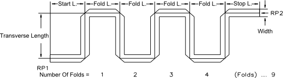
The reference planes are marked RP1 and RP2 in the above diagram. Note, that in order to ease structure definition, the strip center line is used in the above scheme.
The implemented model may consider conductor losses as well as dielectric losses.
The block is characterized by the properties listed below. To modify the values, use the Block Properties – Parameters dialog box. The common substrate properties are defined by a Microstrip Reference Block.
|
Start Length |
Start length from RP1 to the beginning of the folded line (> Width/2) |
|
Stop Length |
Stop length to RP2 (> Width/2) |
|
Transverse Length |
Transverse length of the structure (≥ Height/2 + Width) |
|
Fold Length |
Fold length. The fold length should be ≥ Height/2 + Width for multiple folded lines since the model only considers coupling between adjacent meanders and neglects all other coupling for reasons of efficiency (accuracy reduces if Fold Length < Height/2 + Width). For a single fold, the fold width can be as small as Height/10. |
|
Width |
Width of the trace |
|
Number Of Folds |
Number of folds of the meander (0…9). A value of 0 describes a simple strip displacement (two 90° bends). |
|
Mitered Bends |
Switch that determines the model used for all bends: Either mitered bends with a 50% chamfer or full bends. |
|
Layer |
Index of the reference block layer that is used by the metallization of this block |
The properties listed above and the substrate properties of the reference block define the electrical behaviour of the block. The layout view uses another set of layout properties. These properties define the position of the block in the layout view. The electrical behaviour of the block does not depend on these properties.
See also
Block Overview, Microstrip Reference Block, Layout Properties