|
 Ansoft Designer / Ansys Designer 在线帮助文档: Ansoft Designer / Ansys Designer 在线帮助文档:
Nexxim Simulator >
Nexxim Component Models >
MOSFET Levels 49 through 54 >
BSIM3v3 MOSFET Model, LEVEL=49 and 53
BSIM3v3 MOSFET Model, LEVEL=49 and 53
The syntax for a LEVEL 49 or 53
Berkeley Short-channel IGFET MOSFET (BSIM3v3) model is:
.MODEL modelname NMOS LEVEL=val
[parameter=val] ...
or
.MODEL modelname PMOS LEVEL=val
[parameter=val] ...
modelname is
the name used by MOSFET instances to refer to this .MODEL statement.
LEVEL=49 selects the HSPICEÔ-enhanced BSIM3
model. LEVEL=53 selects the
Berkeley standard BSIM3v3.
Level 49 or 53 MOSFET
Basic Model Parameters
Model Parameter
|
Description
|
Unit
|
Default
|
A0
|
Bulk charge effect coefficient
for channel length
|
None
|
1.0
|
A1
|
1st nonsaturation effect parameter
|
Volt-1
|
0.0
|
A2
|
2nd nonsaturation effect parameter
|
None
|
1.0
|
ACDE
|
Exponential coefficient for charge
thickness in the accumulation and depletion regions (CAPMOD = 3)
|
Meter/Volt
|
1.0
|
AGS
|
Gate bias coefficient of ABULK
|
Volt-1
|
0.0
|
ALPHA0
|
1st parameter of impact ionization
current
|
Meter/Volt
|
0.0
|
ALPHA1
|
Substrate current parameter
|
Volt-1
|
0.0
|
B0
|
Bulk charge coefficient for channel
width
|
Meter
|
0.0
|
B1
|
Bulk charge effect width offset
|
Meter
|
0.0
|
BETA0
|
2nd parameter of impact ionization
current
|
Volt-1
|
30
|
CDSC
|
Drain-source to channel coupling
capacitance
|
Farad/Meter2
|
2.4e-4
|
CDSCB
|
Body-bias sensitivity coefficient
of CDSC
|
Farad/Volt-Meter2
|
0.0
|
CDSCD
|
Drain bias sensitivity of CDSC
|
Farad/Volt-Meter2
|
0.0
|
CIT
|
Interface trap capacitance
|
Farad/Meter2
|
0.0
|
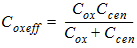
COX
|
Oxide capacitance
|
Farad
|
Calculated
|
DELTA
|
Parameter for DC VDSeff
|
Volt
|
0.01
|
DL (XL)
|
Channel length shortening
|
Meter
|
0.0
|
DROUT
|
Channel length dependence of DIBL
effect on ROUT
|
None
|
0.56
|
DSUB
|
DIBL coefficient in subthreshold
region
|
None
|
DROUT
|
DVT0
|
1st short channel coefficient for
VTH
|
None
|
2.2
|
DVT0W
|
1st narrow width coefficient for
VTH at small L
|
None
|
0.0
|
DVT1
|
2nd short channel coefficient for
VTH
|
None
|
0.53
|
DVT1W
|
2nd narrow width coefficient for
VTH at small L
|
Meter-1
|
5.3e+6
|
DVT2
|
Body-bias coefficient of short
channel effect on VTH
|
Volt-1
|
-0.032
|
DVT2W
|
3rd narrow width coefficient for
VTH at small L
|
Volt-1
|
-0.032
|
DW (XW,
WDEL)
|
Channel width narrowing
|
Meter
|
0.0
|
EG
|
Energy gap for PN junction diode
|
electron-Volt
|
TLEV=0 or 1: 1.11
TLEV=2: 1.16
|
ETA0
|
Subthreshold region DIBL coefficient
|
None
|
0.08
|
ETAB
|
Body-bias coefficient for the subthreshold
DIBL effect
|
Volt-1
|
-0.07
|
GAP1
|
1st bandgap correction factor
|
eV/°K
|
7.02e-4
|
GAP2
|
2nd bandgap correction factor
|
°K
|
1108
|
GEO
|
Shared geometry parameter
|
None
|
0.0
|
HDIF
|
Length of heavily-doped diffusion
|
Meter
|
0.0
|
IJTH
|
Diode limiting current
[Not binnable]
|
Amp
|
0.1
|
K1
|
1st-order body bias factor
|
Amp/Meter
|
0.53
|
K2
|
2nd-order body bias factor
|
None
|
-0.0186
|
K3
|
Narrow width coefficient
|
None
|
80.0
|
K3B
|
Body effect coefficient of K3
|
Volt-1
|
0.0
|
KETA
|
Body-bias coefficient of bulk charge
effect
|
Volt-1
|
-0.047
|
LD (DLAT,
LATD)
|
Lateral diffusion
|
Meter
|
Calculated
|
LDIF
|
Length of lightly-doped region
adjacent to gate
|
Meter
|
0.0
|
MOIN
|
Gate bias-dependent surface potential
coefficient
|
None
|
15.0
|
NCH (NPEAK)
|
Peak doping concentration near
interface
If NCH not specified and GAMMA is specified, NCH
is calculated from GAMMA
|
cm-3
|
1.7e+17
(or calculated)
|
NFACTOR
|
Subthreshold region swing factor
|
None
|
1.0
|
NGATE
|
Poly gate doping concentration
|
cm-3
|
0.0
|
NI
|
Intrinsic concentration
|
cm-3
|
Calculated
|
NLX
|
Lateral nonuniform doping along
channel
|
Meter
|
1.74e-7
|
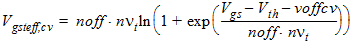
NOFF
|
C-V parameter in VGSTeff, CV for
weak-to-strong inversion transition
|
None
|
1.0
|
NSUB
|
Substrate doping concentration
|
cm-3
|
6.0e+16
|
PCLM
|
Channel length modulation parameter.
|
None
|
1.3
|
PDIBLC1 (PDIBL1)
|
Parameter for DIBL effect on ROUT
|
None
|
0.39
|
PDIBLC2 (PDIBL2)
|
Parameter for DIBL effect on ROUT
|
None
|
0.0086
|
PDIBLCB (PDIBLB)
|
Body bias coefficient of DIBL effect
on ROUT
|
Volt-1
|
0.0
|
PRWB
|
Body effect coefficient of RDSW
|
1/Volt½
|
0.0
|
PRWG
|
Gate bias effect coefficient of
RDSW
|
Volt-1
|
0.0
|
PSCBE1
|
1st substrate current-induced body
effect parameter
|
Volt/Meter
|
4.24e+8
|
PSCBE2
|
2nd substrate current-induced body
effect parameter
|
Meter/Volt
|
1.0e-5
|
PVAG
|
Gate dependence of Early voltage
|
None
|
0.0
|
RD
|
Drain resistance
|
Ohm
|
0.0
|
RDC
|
Additional drain contact resistance
|
Ohm
|
0.0
|
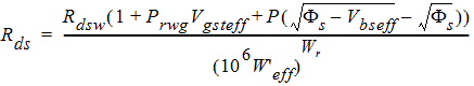
RDSW
|
Parasitic source-drain resistance
per unit width
|
Ohm/mMeterWR
|
0.0
|
RS
|
Source resistance
|
Ohm
|
0.0
|
RSC
|
Additional source contact resistance
|
Ohm
|
0.0
|
RSH
|
Source/drain sheet resistance per
square. [Not binnable]
|
Ohm/square
|
0.0
|
SCALM
|
Scale factor for model parameters
|
None
|
1.0 (or global SCALM option)
|
TNOM (TREF)
|
Temperature at which parameters
are extracted
|
°C
|
25
|
TOX
|
Gate oxide thickness
|
Meter
|
1.50e-8
|
TOXM
|
Reference gate oxide thickness
|
Meter
|
TOX
|
U0
|
Low field mobility at T = TREF
= TNOM
|
cm2/Volt-sec
|
NMOS: 670
PMOS: 250
|
UA
|
1st-order mobility degradation
coefficient
|
Meter/Volt
|
2.25e-9
|
UB
|
2nd-order mobility degradation
coefficient
|
Meter2/Volt2
|
5.87e-19
|
UC
|
Body bias sensitivity coefficient
of mobility
|
MOBMOD=1, 2: Meter/Volt2
MOBMOD=3: Volt-1
|
MOBMOD=1, 2:
-4.65e-11
MOBMOD=3:
-0.0465
|
VBM
|
Maximum substrate bias, for VTH
calculation
|
Volt
|
-3.0
|
VFB
|
DC flatband voltage
|
Volt
|
-1.0
|
VOFF
|
Offset voltage in subthreshold
region at large W and L
|
Volt
|
-0.08
|
VOFFCV
|
C-V parameter in VGSTeff, CV for
weak-to-strong inversion transition
|
None
|
0.0
|
VSAT
|
Saturation velocity of carrier
at T = TREF = TNOM
|
Meter/sec
|
8.0e+4
|
VTH0 (VTHO)
|
Threshold voltage of long-channel
device at VBS=0 and large L
|
Volt
|
Calculated
|
WMLT
|
Width diffusion shrink reduction
factor
|
None
|
1.0
|
W0
|
Narrow width effect coefficient
|
Meter
|
2.5e-6
|
WR
|
Width offset from Weff for RDS
calculation
|
None
|
1.0
|
XJ
|
Junction depth
|
Meter
|
1.5e-7
|
Notes on BSIM3v3 Binning Adjustment
Binning is a way to extend a single device architecture
by providing systematic variations on the device parameters. The philosophy
is that when you vary the channel geometry, other parameters also change,
in ways that can be completely characterized by the device manufacturer.
The manufacturer or foundry provides a “design kit” that
contains a set of .MODEL statements specifying the parameter settings
for the different geometries. The design kit with the .MODEL statements
can be included in the Nexxim design as a subcircuit.
1. A binning model is identified by giving the
model name in the .MODEL statement the form modelname.n,
where the entry n after the decimal point can be an integer or
any other unique identifier. The MOSFET instance definition refers to
the modelname without any extension. The netlist can contain
any number of different binning models with the same base modelname.
For example, three binning models could be named NMOSBSIM3.1 NMOSBSIM3.2,
and NMOSBSIM3.3. The instance statement would reference simply NMOSBSIM3.
Each of the available binning models corresponds
to a range of channel lengths and widths specified with the LMIN,
LMAX, WMIN, and WMAX model parameters. The ranges
must not overlap.
Each binning model typically specifies values
for the model parameters that are related to the channel geometry variations.
2. The MOSFET instance statement must contain values
for instance parameters L and W. The L and W
parameters can be specified with variables so that a sweep of binning
models can be performed.
3. The simulator finds the binning model to which
the following conditions BOTH apply:
• The LMIN and LMAX model
parameter range includes the value of instance parameter L (scaled
by the instance parameter SCALE).
• The WMIN and WMAX model
parameter range includes the value of instance parameter W (scaled
by the instance parameter SCALE).
If none of the available binning models matches
the L and W instance parameters, simulation does not proceed.
4. Within a BSIM3v3 model, (binned or not) the binned
model parameters are adjusted by the effective channel length and width.
The formulas for the adjustment use the following symbols:
N = value of the model parameter, for example
A0.
LN = value of the length dependence parameter,
for example LA0.
WN = value of the width dependence parameter,
for example WA0.
PN = value of the cross dependence parameter,
for example PA0.
Leff = effective channel length (calculated
from L using scale factors and other adjustments).
Weff = effective channel width (calculated
from W using scale factors and other adjustments).
LREFeff = effective reference channel length
(calculated from model parameter LREF using scale factors and
other adjustments).
WREFeff = effective reference channel width
(calculated from WREF using scale factors and other adjustments).
When model parameter BINFLAG is greater
than 0.9 AND the model parameters LREF and WREF are both
greater than 0:
Value = N + LN*(1/Leff-1/LREFeff)
+ WN*(1/Weff-1/WREFeff)
+ PN*(1/(Leff-1/LREFeff)*(1/(Weff-1/WREFeff)))
Otherwise:
Value = N + LN*(1/Leff) + WN*(1/Weff) + PN*(1/(Leff*Weff))
5. When model parameter BINUNIT equals 1,
the effective parameters (Leff, Weff, LREFeff, and WREFeff) are scaled
to units of microns. By default (BINUNIT not equal to 1), units
are meters.
The unit for the length dependence parameters
is the unit of the basic parameter divided by Meter.
Level 49 or 53 Length
Dependence Parameters
Model Parameter
|
Description
|
Default
|
La0
|
Length dependence of a0
|
0.0
|
La1
|
Length dependence of a1
|
0.0
|
La2
|
Length dependence of a2
|
0.0
|
Lacde
|
Length dependence of acde
|
0.0
|
Lags
|
Length dependence of ags
|
0.0
|
Lalpha0
|
Length dependence of alpha0
|
0.0
|
Lalpha1
|
Length dependence of alpha1
|
0.0
|
Lat
|
Length dependence of at
|
0.0
|
Lb0
|
Length dependence of b0
|
0.0
|
Lb1
|
Length dependence of b1
|
0.0
|
Lbeta0
|
Length dependence of beta0
|
0.0
|
Lcdsc
|
Length dependence of cdsc
|
0.0
|
Lcdscb
|
Length dependence of cdscb
|
0.0
|
Lcdscd
|
Length dependence of cdscd
|
0.0
|
Lcf
|
Length dependence of cf
|
0.0
|
Lcgdl
|
Length dependence of cgdl
|
0.0
|
Lcgsl
|
Length dependence of cgsl
|
0.0
|
Lcit
|
Length dependence of cit
|
0.0
|
Lckappa
|
Length dependence of ckappa
|
0.0
|
Lclc
|
Length dependence of clc
|
0.0
|
Lcle
|
Length dependence of cle
|
0.0
|
Ldelta
|
Length dependence of delta
|
0.0
|
Ldrout
|
Length dependence of drout
|
0.0
|
Ldsub
|
Length dependence of dsub
|
0.0
|
Ldvt0
|
Length dependence of dvt0
|
0.0
|
Ldvt0w
|
Length dependence of dvt0w
|
0.0
|
Ldvt1
|
Length dependence of dvt1
|
0.0
|
Ldvt1w
|
Length dependence of dvt1w
|
0.0
|
Ldvt2
|
Length dependence of dvt2
|
0.0
|
Ldvt2w
|
Length dependence of dvt2w
|
0.0
|
Ldwb
|
Length dependence of dwb
|
0.0
|
Ldwg
|
Length dependence of dwg
|
0.0
|
Lelm
|
Length dependence of elm
|
0.0
|
Leta0
|
Length dependence of eta0
|
0.0
|
Letab
|
Length dependence of etab
|
0.0
|
Lgamma1
|
Length dependence of gamma1
|
0.0
|
Lgamma2
|
Length dependence of gamma2
|
0.0
|
Lk1
|
Length dependence of k1
|
0.0
|
Lk2
|
Length dependence of k2
|
0.0
|
Lk3
|
Length dependence of k3
|
0.0
|
Lk3b
|
Length dependence of k3b
|
0.0
|
Lketa
|
Length dependence of keta
|
0.0
|
Lkt1
|
Length dependence of kt1
|
0.0
|
Lkt1l
|
Length dependence of kt1l
|
0.0
|
Lkt2
|
Length dependence of kt2
|
0.0
|
Lmoin
|
Length dependence of moin
|
0.0
|
Lnch (Lnpeak)
|
Length dependence of nch
|
0.0
|
Lnfactor
|
Length dependence of nfactor
|
0.0
|
Lngate
|
Length dependence of ngate
|
0.0
|
Lnlx
|
Length dependence of nlx
|
0.0
|
Lnoff
|
Length dependence of noff
|
0.0
|
Lnsub
|
Length dependence of nsub
|
0.0
|
Lpclm
|
Length dependence of pclm
|
0.0
|
Lpdibl1
|
Length dependence of Pdibl1
|
0.0
|
Lpdibl2
|
Length dependence of Pdibl2
|
0.0
|
Lpdiblb
|
Length dependence of Pdiblb
|
0.0
|
Lprt
|
Length dependence of prt
|
0.0
|
Lprwb
|
Length dependence of prwb
|
0.0
|
Lprwg
|
Length dependence of prwg
|
0.0
|
Lpscbe1
|
Length dependence of pscbe1
|
0.0
|
Lpscbe2
|
Length dependence of pscbe2
|
0.0
|
Lpvag
|
Length dependence of pvag
|
0.0
|
Lrdsw
|
Length dependence of rdsw
|
0.0
|
Lu0
|
Length dependence of u0
|
0.0
|
Lua
|
Length dependence of ua
|
0.0
|
Lua1
|
Length dependence of ua1
|
0.0
|
Lub
|
Length dependence of ub
|
0.0
|
Lub1
|
Length dependence of ub1
|
0.0
|
Luc
|
Length dependence of uc
|
0.0
|
Luc1
|
Length dependence of uc1
|
0.0
|
Lute
|
Length dependence of ute
|
0.0
|
Lvbm
|
Length dependence of vbm
|
0.0
|
Lvbx
|
Length dependence of vbx
|
0.0
|
Lvfb
|
Length dependence of vfb
|
0.0
|
Lvfbcv
|
Length dependence of vfbcv
|
0.0
|
Lvoff
|
Length dependence of voff
|
0.0
|
Lvoffcv
|
Length dependence of voffcv
|
0.0
|
Lvsat
|
Length dependence of vsat
|
0.0
|
Lvth0
|
Length dependence of vth0
|
0.0
|
Lw0
|
Length dependence of w0
|
0.0
|
Lwr
|
Length dependence of wr
|
0.0
|
Lxj
|
Length dependence of xj
|
0.0
|
Lxt
|
Length dependence of xt
|
0.0
|
The unit for the width dependence parameters
is the unit of the basic parameter divided by Meter.
The unit for cross dependence parameters
is the unit of the basic parameter divided by Meter2.
BSIM3v3 MOSFET Model Netlist Examples
.model nenh nmos
+Level=49 VERSION=3.22
+Tnom=27.0 capmod=3 paramchk=0 mobmod=1
+Nch=1e+16 Tox=5E-08 Xj=3.85E-08
+Lint=9.36e-8 Wint=0
+Vth0= .779 K1=1.04 K2= -3.83e-2 K3=50
+Dvt0= 2.812 Dvt1= 0.462 Dvt2=-9.17e-2
+Nlx= 3.52291E-08 W0= 1.163e-6
+K3b= 2.233
+Vsat= 86301.58 Ua= 6.47e-9 Ub= 4.23e-18 Uc=-4.706281E-11
+U0=400 wr=1
+A0= .3496967 Ags=.1 B0=0.546 B1= 1
+ Dwg = -6.0E-09 Dwb = -3.56E-09 Prwb = -.213
+Keta=-3.605872E-02 A1= 2.778747E-02 A2= .9
+Voff=-6.735529E-02 NFactor= 1.139926 Cit= 1.622527E-04
+cj=0.00042 mj=0.5 pb=1.0
+cjsw=9e-12 mjsw=0.33 pbsw=1.0
+cjswg=9e-12 mjswg=0.33 pbswg=1.0
+cgsl=5.0e-10 ckappa=0.6
+cgdl=3.6e-10
+cf=0.0 cgso=5.2e-10 cgdo=5.2e-10
+cgbo=4.0e-10
+Cdsc=2.4e-4
+Cdscb= 0 Dvt0w = 0 Dvt1w = 0 Dvt2w = 0
+Cdscd = 0 Prwg = 0
+dlc=9.36e-8 dwc=0.0
+Eta0= 1.0281729E-02 Etab=-5.042203E-03
+Dsub= .31871233
+Pclm= 1.114846 Pdiblc1= 2.45357E-03 Pdiblc2= 6.406289E-03
+Drout= .31871233 Pscbe1= 5000000 Pscbe2= 5E-09
+Pdiblcb = -.234
+Pvag= 0 delta=0.01
+Wl = 0 Ww =0 Wwl = 0
+Wln = 0 Wwn = .2613948 Ll =0.0
+Lw = 0 Lwl = 0 Lln = .316394
+Lwn = 0
+kt1=-.3 kt2=-.051
+At= 22400
+Ute=-1.48
+Ua1= 3.31E-10 Ub1= 2.61E-19 Uc1= -3.42e-10
+Kt1l=0 Prt=764.3
+xpart=0.2
+JS =1e-2 JSW=0
+VFBCV=-1 VFB=-1
BSIM3v3.3 Model Equations
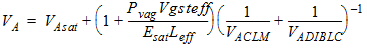
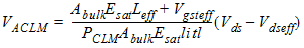
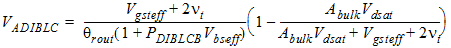
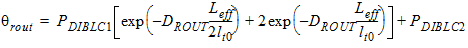
1. I-V Model Equations
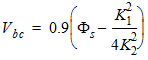
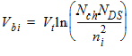
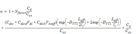
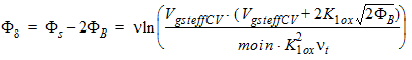
1.1 Threshold Voltage
![[spacer]](1p.gif)
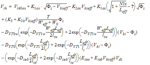
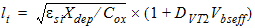
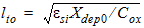
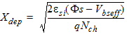
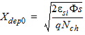

d1=0.001
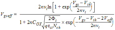
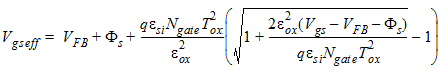
1.2 Effective (Vgs-Vth)

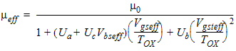
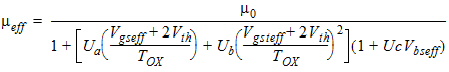
1.3 Mobility
For MOBMOD = 1:

For MOBMOD = 2:
For MOBMOD = 3:
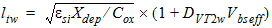
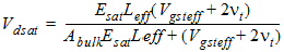
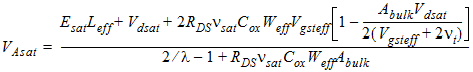
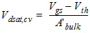
1.4 Drain Saturation Voltage
For Rds >
0 or l ¹ 1:
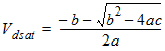
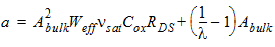


l
= A1Vgsteff + A2
For Rds =
0 and l = 1:


1.5 Effective Vds

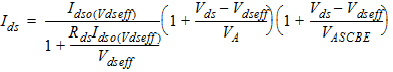
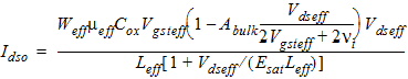
1.6 Drain Current Expression
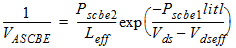
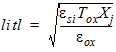
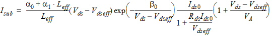
1.7 Substrate Current
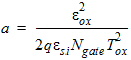
1.8 Polysilicon Depletion Effect
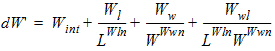
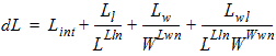
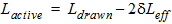
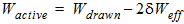
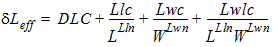
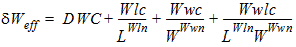
1.9 Effective Channel Length and Width
Leff = Ldrawn - 2dL
Weff = Wdrawn - 2dW
W'eff = Wdrawn - 2dW'

1.10 Source/Drain Resistance
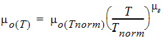
1.11 Temperature Effects


2. Capacitance Model Equations
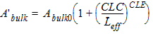
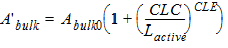
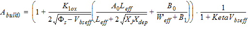
2.1 Dimension Dependence
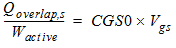
2.2 Overlap Capacitance
2.2.1 Source Overlap Capacitance
2.2.1.1 For CAPMOD = 0:
2.2.1.2 For CAPMOD = 1
2.2.1.2.1 For Vgs
< 0:
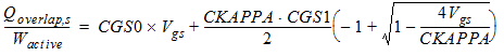
2.2.1.2.2 For Vgs ³
0:
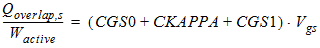
2.2.1.3 For CAPMOD = 2


2.2.2 Drain Overlap Capacitance
2.2.2.1 For CAPMOD = 0:
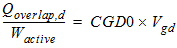
2.2.2.2 For CAPMOD = 1
2.2.2.2.1 If Vgd
< 0:
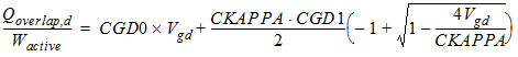
2.2.2.2.2 If Vgd
³ 0:
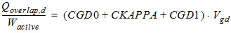
2.2.2.3 For CAPMOD = 2:


2.2.3 Gate Overlap Charge
2.3 Intrinsic Charges:
2.3.1 For CAPMOD = 0
2.3.1.1 Accumulation Region (Vgs
< Vfbcv + Vbs)

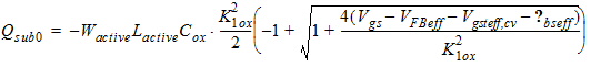
Qsub = -Qg
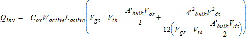
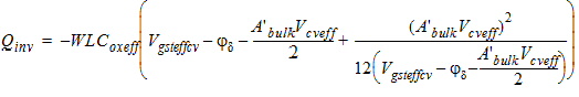
Qinv = 0
2.3.1.2 Subthreshold Region (Vgs
< Vth)
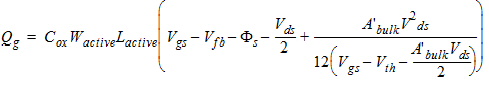
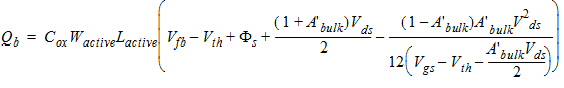
Qg
= -Qb
Qinv = 0
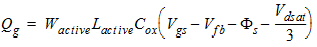
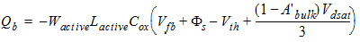
2.3.1.3 Strong Inversion Region (Vgs > Vth)

2.3.1.3.1 50/50 Charge Partition
2.3.1.3.1.1 If Vds
< Vdsat
2.3.1.3.1.2 Else (Vds
³ Vdsat)


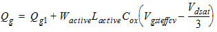
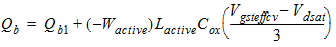
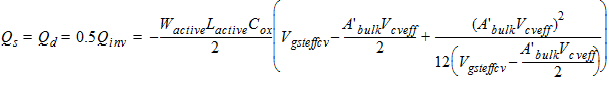
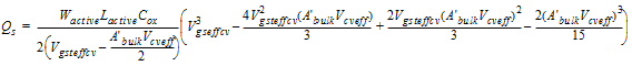
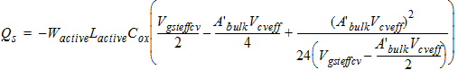
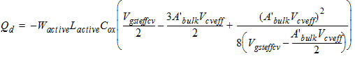
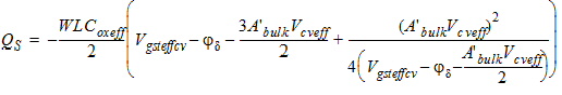
2.3.1.3.2 Strong Inversion Region (Vgs > Vth):
40/60 Charge Partition
2.3.1.3.2.1 If Vds
< Vdsat

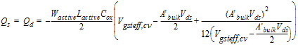
Qs
= -(Qg + Qb + Qd)
2.3.1.3.2.2 Else (Vds
³ Vdsat)

Qs
= -(Qg + Qb + Qd)

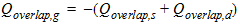
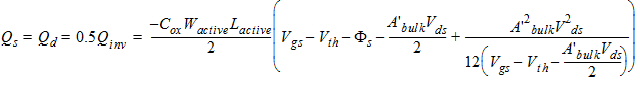
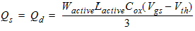
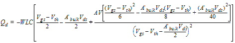
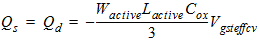
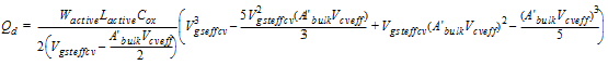
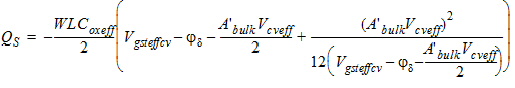
2.3.1.3.3 Strong Inversion Region (Vgs > Vth):
0/100 Charge Partition
2.3.1.3.3.1 If Vds
< Vdsat


Qs
= -(Qg + Qb + Qd)
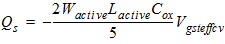
2.3.1.3.3.2 Else (Vds
³ Vdsat)
Qs
= -(Qg + Qb)
Qd
= 0
2.3.2 CAPMOD = 1
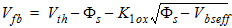
2.3.2.1 Flatband Voltage

Note
|
The bias dependencies
given for the threshold voltage Vth
in the I-V Model Equations section are not considered in calculating
the flatband voltage Vfb for
CAPMOD=1.
|
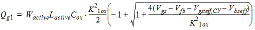
2.3.2.2 If (Vgs
< Vfb + Vbs + Vgsteffcv)
Qg1
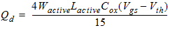
= WactiveLactiveCox(Vgs - Vfb -Vbs -Vgsteffcv)
2.3.2.3 If (Vgs
³ Vfb + Vbs + Vgsteffcv)
Qb1
= -Qg1


2.3.2.4 If (Vds £ Vdsat)
2.3.2.4.1 50/50 Channel-charge Partition
2.3.2.4.2 40/60 Channel-charge Partition

Qd
= -(Qg + Qb + Qs)
2.3.2.4.3 0/100 Channel-charge Partition
Qd
= -(Qg + Qb + Qs)
2.3.2.5 If (Vds
> Vdsat)
2.3.2.5.1 50/50 Channel-charge Partition
2.3.2.5.1 40/60 Channel-charge Partition
Qd
= -(Qg + Qb + Qs)
2.3.2.5.1 0/100 Channel-charge Partition
Qd
= -(Qg + Qb + Qs)
2.3.3 CAPMOD = 2
Note
|
The bias dependencies
given for the threshold voltage Vth
in the I-V Model Equations section are not considered in calculating
the flatband voltage Vfb for
CAPMOD=2.
|
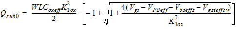
Qg
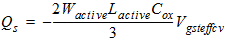
= -(Qinv + Qacc + Qsub0 +dQsub)
Qb
= Qacc + Qsub0 +dQsub
Qinv = Qs + Qd
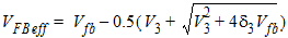
V3
= Vfb-Vgb - d3,
d3 = 0.02
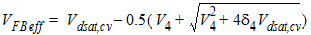
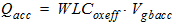
Qacc = -WactiveLactiveCox(VFBeff -Vfb)

V4
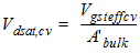
= Vdsat,cv-Vds - d4,
d4 = 0.02
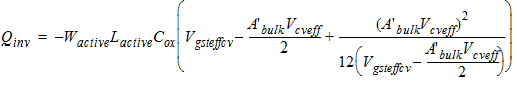
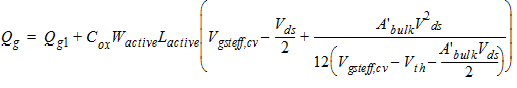
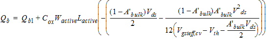
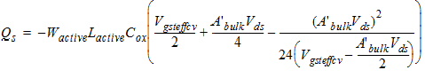
2.3.3.1 50/50 Charge Partition
2.3.3.2 40/60 Channel Partition
2.3.3.3 0/100 Channel Partition
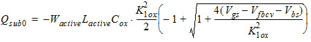
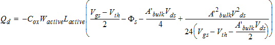
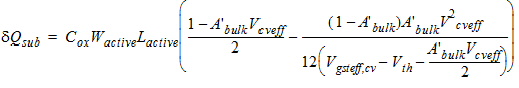
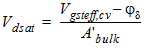
2.3.4 CAPMOD = 3 (Charge-Thickness Model)

Note
|
The bias dependencies
given for the threshold voltage Vth
in the I-V Model Equations section are not considered in calculating
the flatband voltage Vfb for
CAPMOD=3.
|
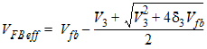
d3 = 0.02
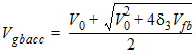
V0
= Vfb + Vfbeff -Vgs -d3
V3
= Vfb + Vbseff -Vgs -d3

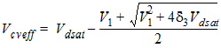
V1
= Vdsat -Vds -d3
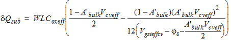
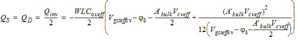
2.3.4.1 50/50 Charge Partition
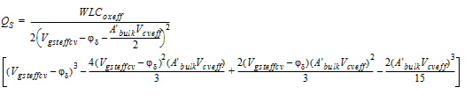
2.3.4.2 40/60 Charge Partition
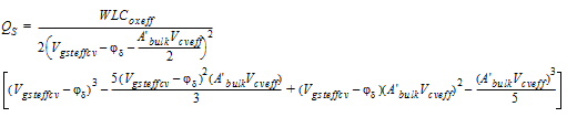
2.3.4.3 0/100 Charge Partition


HFSS视频教程
ADS视频教程
CST视频教程
Ansoft Designer 中文教程
|